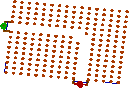
2D photonic crystal waveguide bend
The present example considers a 2D photonic crystal waveguide bend.
2D photonic crystal waveguide bend.
Simulation model considers a sharp 90o bend hollowed in a 2D PhC composed of GaAs rods of radius r = 104 nm distributed with lattice constant a = 580 nm (A.Mekis, J.Chen, I.Kurland, S.Fan, P.Villeneuve, J.Joannopoulos, "High Transmission through Sharp Bends in Photonic Crystal Waveguides", Physical Review Letters, Vol. 77, No. 18, October 1996, pp.3787-3790). Spectrum of a transmitted signal is set in the third telecommunication window at λ = 1550 nm. Proper design of the corner neighbourhood allows us to optimise transmission efficiency.
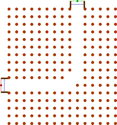
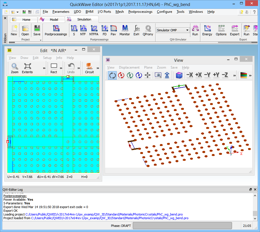
2D photonic crystal waveguide bend project in QW-Editor.
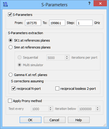
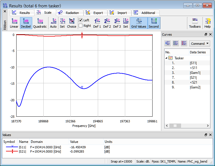
For the purpose of calculating reflection and transmission characteristics of the structure, the S-Parameters postprocessing is activated. The S-Parameters postprocessing is set from 187370 GHz to 199861 GHz with a frequency step of 1 GHz.
S-Parameters postprocessing configuration dialogue.
Reflection and transmission characteristics of the photonic crystal wavguide bend.
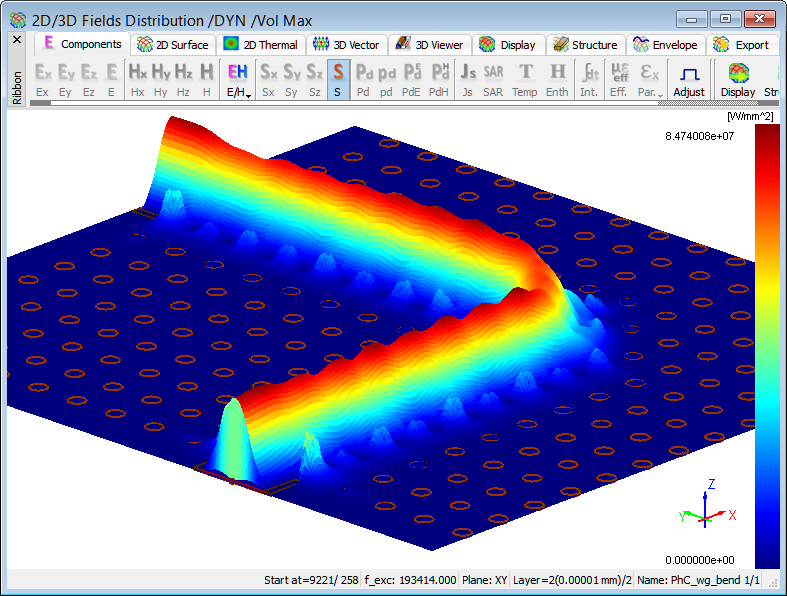
Distribution of time-maximum envelope of Poynting vector at 193.414 THz (λ = 1550 nm).
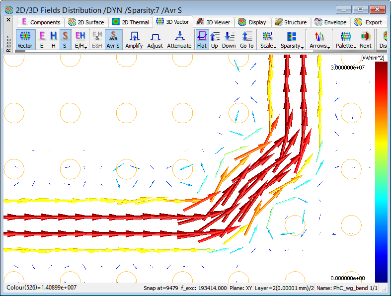
Vector display of time-maximum envelope of Poynting vector at 193.414 THz (λ = 1550 nm).