2.18.1 2D photonic crystal waveguide
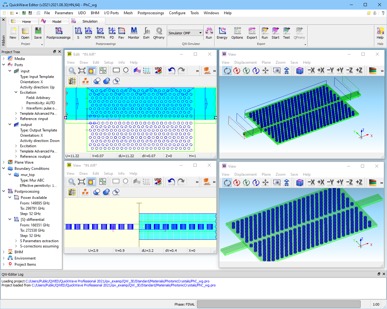
Let us consider planar photonic waveguide manufactured in a 2D hexagonal PhC designed for the purpose of the third telecommunication window [M5]. Fig. 2.18.1-1 shows geometry of the considered PhC waveguide manufactured in 200 nm thick Si wafer (n = 3.26) with air cladding. In principle, photonic crystal lattice (a = 390 nm) surrounding waveguide region is composed of the air holes of radius r = 107 nm. TE polarisation (electric field parallel to the wafer plane) exhibits a photonic bandgap (PBG) inside the PhC region around 1.4μm wavelength. Line defect operating as a PhC waveguide is about 6 μm wide and 10 μm long. Due to symmetry of the excited mode and structure, we can reduce the size of the model imposing electric symmetry in the middle of the waveguide width.
Fig. 2.18.1-1 Photonic crystal waveguide considered in PhC_wg.pro.
Fig. 2.18.1-2 shows calculated transmission coefficient in the 1.1 – 1.8 μm wavelength range. We can notice that the passband is mainly between 1.2 and 1.45 μm, corresponding to the PBG of the applied PhC.
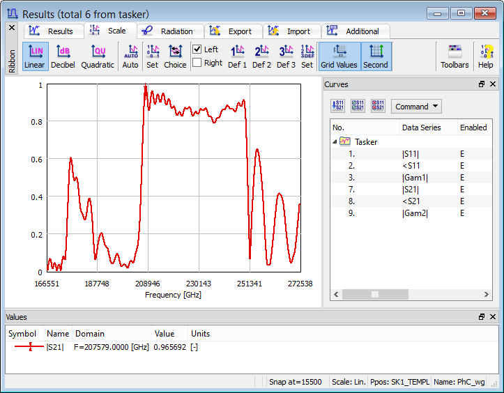
Fig. 2.18.1-2 Transmission coefficient spectrum (power scaling).
Fig. 2.18.1-3 presents envelope of the magnetic field at f = 207579 GHz (λ = 1.44 μm). It can be seen that the field is concentrated near the waveguide region and only a few PhC rows are needed to guide the light properly.
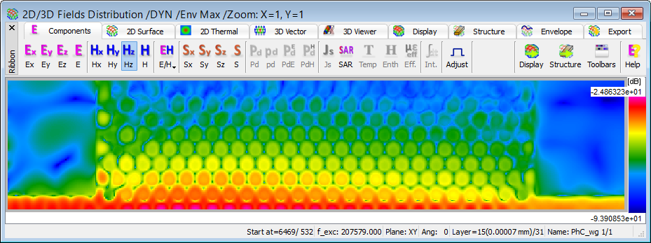
Fig. 2.18.1-3 Envelope of the magnetic field in the decibel scale.