2.18.2 2D photonic crystal waveguide bend
Another example depicts a unique advantage of PhC waveguide very difficult to obtain in waveguiding structures with strict boundary conditions. As shown in the Fig. 2.18.2-1, we consider a sharp 90° bend hollowed in a 2D PhC composed of GaAs rods of radius r = 104 nm distributed with lattice constant a = 580 nm [M4]. Spectrum of a transmitted signal is set in the third telecommunication window at λ = 1550 nm. Proper design of the corner neighbourhood allows us to optimise transmission efficiency.
Fig. 2.18.2-1 Sharp bend in the PhC waveguide considered in PhC_wg_bend.pro.
The Fig. 2.18.2-2 depicts obtained scattering parameters around frequency of our interest f = 193414 GHz (λ = 1550 nm). It can be noticed that the transmission coefficient is about |S21| = ‑0.1 dB providing ~98% of injected energy to the output. Envelope of the Poynting vector calculated at this frequency (see Fig. 2.18.2-3) clearly indicates that energy is very well concentrated in a waveguiding defect penetrating interior of PhC only a little.
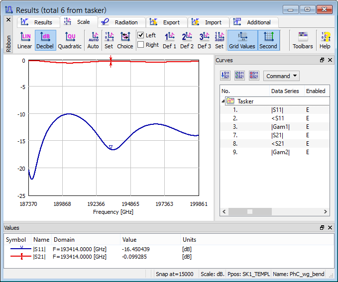
Fig. 2.18.2-2 Scattering parameters obtained in the PhC_wg_bend.pro.
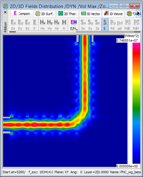
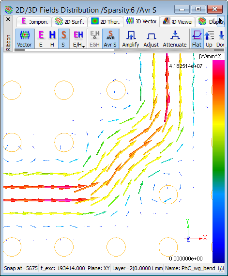
Fig. 2.18.2-3 Envelope of Poynting vector obtained in the PhC_wg_bend.pro at λ = 1550 nm.