2.2.11 Salisbury screen absorber
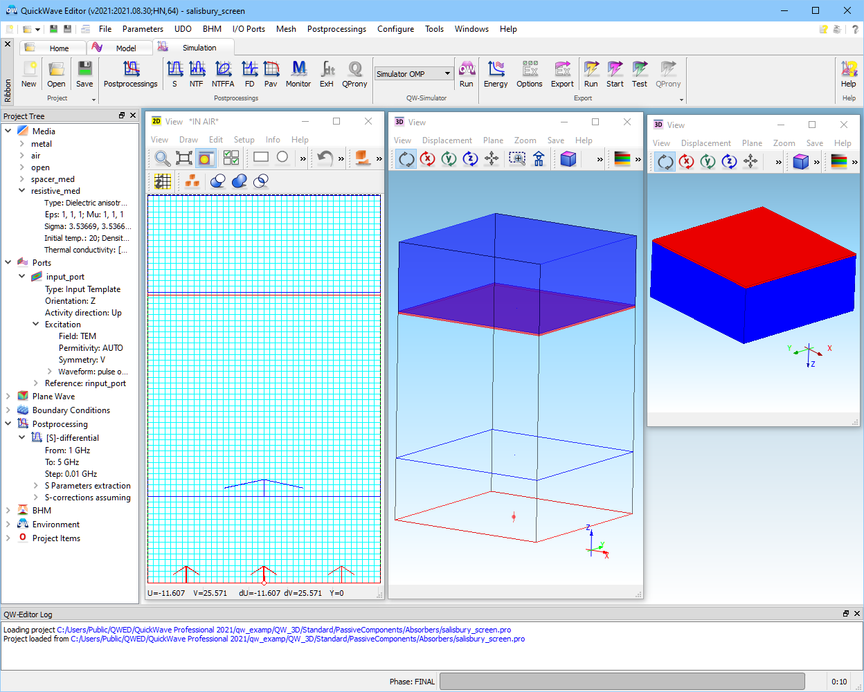
We shall consider one of the most popular absorbing structures called Salisbury screen, described by ..\PassivieComponents\Absorbers\salisbury_screen.pro. Fig. 2.2.11-1shows the absorber in 2Dand 3D Windows in QW-Editor. We assume that the structure is infinite and we are analysing only a small part of it to speed up the calculations.
In general, the Salisbury screen operating at frequency f1, consists of a quarter-wavelength thick (at f1) lossless dielectric spacer and a resistive sheet with a surface resistance equal to the impedance of a free space. At an operating frequency the Salisbury screen becomes quasi-matched to a free space, what facilitates the energy dissipation in the resistive sheet.
Here we consider the Salisbury screen operating at 3 GHz with a 25 mm thick air spacer and will investigate its reflection coefficient in the frequency range from 1 GHz to 5 GHz.
Fig. 2.2.11-1 QW-Editor display of the salisbury_screen.pro example.
The structure is meshed using manual meshing option (Mesh Parameters dialogue). The mesh settings are shown in Fig. 2.2.11-2. The maximum cell size is set to 1.5 mm in all directions, what corresponds to 40 cells per wavelength at the highest frequency of the considered bandwidth in a vacuum.

Fig. 2.2.11-2 The Mesh Parameters dialogue.
The material parameters are set via Project Media dialogue. After choosing resistive_med from the media list the setting as shown in Fig. 2.2.11-3 will appear. What may cause some doubts, is the medium Type chosen to be Dielectric anisotropic instead of lossy metal, as probably expected. Let us shortly explain this choice. When considering lossy metals the skin depth is very small and in microwave frequency range it does not exceed several micrometers. If we wanted to model the wave evanescing exponentially in such material, it would require introducing a sub-micrometer cells, what will extremely prolong the simulation time. For that reason, in QuickWave we assume that even thin metal layer is non-transparent and the losses are taken into account by assigning them to the tangential magnetic field in the metal neighbourhood. In Salisbury screen, by definition, the resistive sheet is assumed to be partially transparent and thus the lossy metal model is not adequate for this case. Thus we assume that the lossy medium is dielectric with a finite conductivity. If the medium was assumed to be an isotropic, the properties of the real thin resistive sheet in the normal direction would be mapped improperly. Thus we use an anisotropic model.
By definition the surface resistance of the resistive sheet in Salisbury screen is equal 377 Ω/□ and the sheet is very thin. The assumption concerning the sheet thickness can become problematic when creating FDTD model, because it will introduce a very small cell, which will cause a significant drop down of a FDTD time step and simulation slow down. When creating a simulation model we can introduce an equivalent sheet with a higher thickness and the conductivity defined according to:
![]() ,
,
where Rs is a required surface resistance and t is a sheet model thickness. In the considered scenario we use 0.75 mm thick resistive sheet with a surface resistance of 377 Ω/□, what gives an equivalent conductivity of ca. 3.54 [S/m], as shown in Fig. 2.2.11-3. Please also note that the resistive layer have a half-cell thickness.

Fig. 2.2.11-3 Project Media dialogue with resistive sheet material parameters.
The structure has been illuminated with a plane wave in the frequency range from 1 to 5 GHz. The excitation parameters for the input port has been shown in Fig. 2.2.11-4.

Fig. 2.2.11-4 Edit Transmission Line Port dialogue with project excitation.
Fig. 2.2.11-5shows the S-Parametersdialogue with S-Parameters post-processing settings for the considered example. We are interested in obtaining S-parameters in the frequency range 1 ÷ 5 GHz.

Fig. 2.2.11-5 S-Parameters dialogue for the considered project.
The reflection coefficient for the considered Salisbury screen is shown in Fig. 2.2.11-6. As you can see at the operating frequency we obtain very good absorber’s performance (-60dB). From the obtained results we can confirm the main feature of the Salisbury screens, which is a narrow operating bandwidth (relative bandwidth, calculated with respect to centre frequency, measured at the level of -20dB equals 25%).

Fig. 2.2.11-6 The results of analysis of |S11| of salisbury_screen.pro.
Let us now point out a significant meshing issue, when analysing structures containing thin lossy sheets. The meshing scenario in the neighbourhood of lossy sheet becomes very significant, when defining its effective distance from the reflecting surface. Let us consider the case of salisbury_screen.pro. We have introduced a lossy sheet of a half-cell thickness. To assure proper EM field calculations we should enforce a mesh snapping plane at upper or lower sheet surface (in Z direction). The answer to a question where to put the special plane? is essential for further calculations. In the salisbury_screen.pro we utilise the meshing scenario on the left in Fig. 2.2.11-7. According to Fig. 2.2.11-6 the operating frequency is as expected 3 GHz. Let us now consider the structure, where meshing scenario on the right in Fig. 2.2.11-7is adopted. For that purpose load salisbury_screen1.pro. The difference in the meshing can be easily seen in the 2D Window (in either XZ or YZ plane). The simulation results for salisbury_screen1.pro are presented in Fig. 2.2.11-8. As you can notice, despite the thickness of the spacer has not been changed, the operating frequency of the absorber has shifted down to f2= 2.91GHz.
Let us explain this situation. As mentioned in Electromagnetic fields the Ex component in each cell is calculated at the upper edge of the cell. This implies that for the meshing scenario as in salisbury_screen.pro the losses will be assigned to the cell where the resistive sheet is placed (cell no. 1 in Fig. 2.2.11-7 left) and the effective distance between the reflecting surface and the lossy layer is equal to the thickness of the spacer. Thus, the operating frequency is 3 GHz. In the salisbury_screen1.pro meshing scenario the losses will be assigned to the Ex component of the cell below the resistive sheet (cell no. 1 in Fig. 2.2.11-7right). In such case the effective distance between the reflecting surface and lossy layer corresponds to the sum of spacer thickness and resistive layer thickness, thus in our case 25.75 mm. Assuming λ/4= 25.75 mm the operating frequency of the absorber equals 2.91 GHz, what is confirmed in Fig. 2.2.11-8.
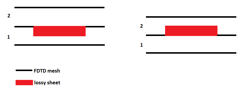
Fig. 2.2.11-7 Two optional meshing scenarios in the lossy sheet neighbourhood.

Fig. 2.2.11-8 The results of analysis of |S11| of salisbury_screen1.pro.
The considered examples show the importance of the applied meshing scenario when analysing structures containing thin lossy sheets like for example microwave absorbers.
As an additive, in Fig. 2.2.11-9we have put several different meshing scenarios in the lossy sheet neighbourhood and have indicated the effective distance from the reflecting object to lossy layer in each of them.

Fig. 2.2.11-9 Different meshing scenarios with effective distance between the conducting surface and lossy layer indicated.