2.3.3 Patch antenna
We consider a circular patch antenna described by the file: ..\Antennas\Patch\patch1.pro. The project is composed of two objects called from standard QW-3D libraries. Please press ![]() to see the list of these objects (marked as UDO objects). They are:
to see the list of these objects (marked as UDO objects). They are:
patch1 - describing a circular patch fed by a thin vertical coax line (generated by a call to ..\antennas\patch1.udo);
NTF - describing the Near-to-Far transformation surface surrounded by six superabsorbing walls (generated by a call to ..\boxes\ntf.udo).
The general 3D view of the structure is presented in Fig. 2.3.3-1.

Fig. 2.3.3-1 General view of the structure of patch1.pro and a fragment of meshing including the cross-section of the coax feed line approximated by a square shape.
As in the case of other antennas, we run the simulation with two types of postprocessings: S-Parameters and Near To Far. The first one calculates the return loss versus frequency. After running the example for about 1200 iterations and invoking Results window (by pressing ![]() button or
button or ![]() button from S-Parameters section in Results tab of QW-Simulator) we obtain the characteristic presented in Fig. 2.3.3-2. We can see the resonances corresponding to the consecutive modes. The cursor indicates one of the modes appearing at the frequency 5.525 GHz. For radiation patterns we will consider this mode as well as the mode appearing at 2.65 GHz.
button from S-Parameters section in Results tab of QW-Simulator) we obtain the characteristic presented in Fig. 2.3.3-2. We can see the resonances corresponding to the consecutive modes. The cursor indicates one of the modes appearing at the frequency 5.525 GHz. For radiation patterns we will consider this mode as well as the mode appearing at 2.65 GHz.
The simulation for more than 12200 iterations has been long enough to make the characteristics of Fig. 2.3.3-2 very smooth. It is worth noting that the resonances of the patch are well visible much faster but there are some ripples on the characteristics. These ripples are not critical to the accuracy of extraction of the desired information, and that is why if the computing time is important, the simulation can be interrupted before they vanish completely (for example at about 6000 iterations).
When choosing the parameters of the considered project in QW-Editor we have assumed (in Near To Far dialogue) that we would be calculating the radiation patterns at 2.65 and 5.525 GHz. When the example is run in QW-Simulator the first click Results button brings the S-parameters display as presented in Fig. 2.3.3-2. To get the radiation patterns we need to invoke Next Postprocessing command from Run tab and then press Results (![]() ) button again or simply press
) button again or simply press ![]() button in 2D Radiation Pattern section of Results tab of QW-Simulator. This brings up the Radiation Patterns window as already considered in Rectangular waveguide horn in open space (see Fig. 2.3.1-5). Let us choose the z-axis as the reference and request the calculation of the radiation patterns versus elevation angle (Theta) with azimuthal angle (Phi) equal to 0 degree. Fig. 2.3.3-3 shows the calculated radiation patterns. At each frequency we display patterns for two polarisations. In both cases the polarisation E[theta] dominates. But it is interesting to note that at 2.65 GHz the radiation is maximum in vertical direction while at 5.525 GHz the radiation in this direction is very small.
button in 2D Radiation Pattern section of Results tab of QW-Simulator. This brings up the Radiation Patterns window as already considered in Rectangular waveguide horn in open space (see Fig. 2.3.1-5). Let us choose the z-axis as the reference and request the calculation of the radiation patterns versus elevation angle (Theta) with azimuthal angle (Phi) equal to 0 degree. Fig. 2.3.3-3 shows the calculated radiation patterns. At each frequency we display patterns for two polarisations. In both cases the polarisation E[theta] dominates. But it is interesting to note that at 2.65 GHz the radiation is maximum in vertical direction while at 5.525 GHz the radiation in this direction is very small.

Fig. 2.3.3-2 |S11| versus frequency indicating several modes of the patch antenna.
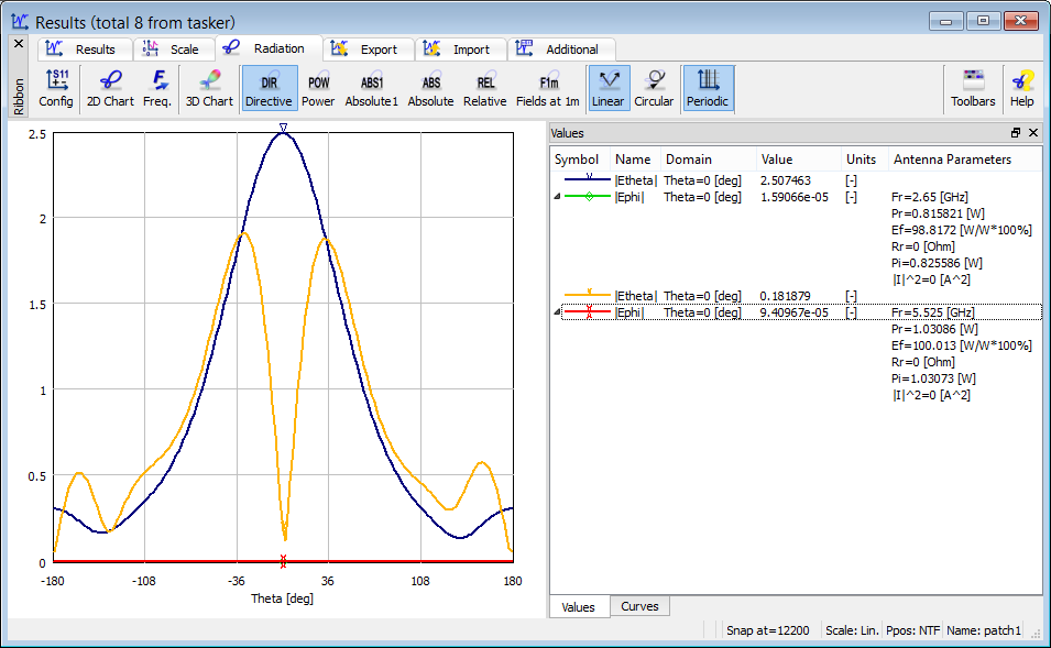
Fig. 2.3.3-3 Radiation patterns versus elevation angle Theta with azimuthal angle Phi=0, calculated in the example patch1.pro for two frequencies: 2.65 and 5.525 GHz.
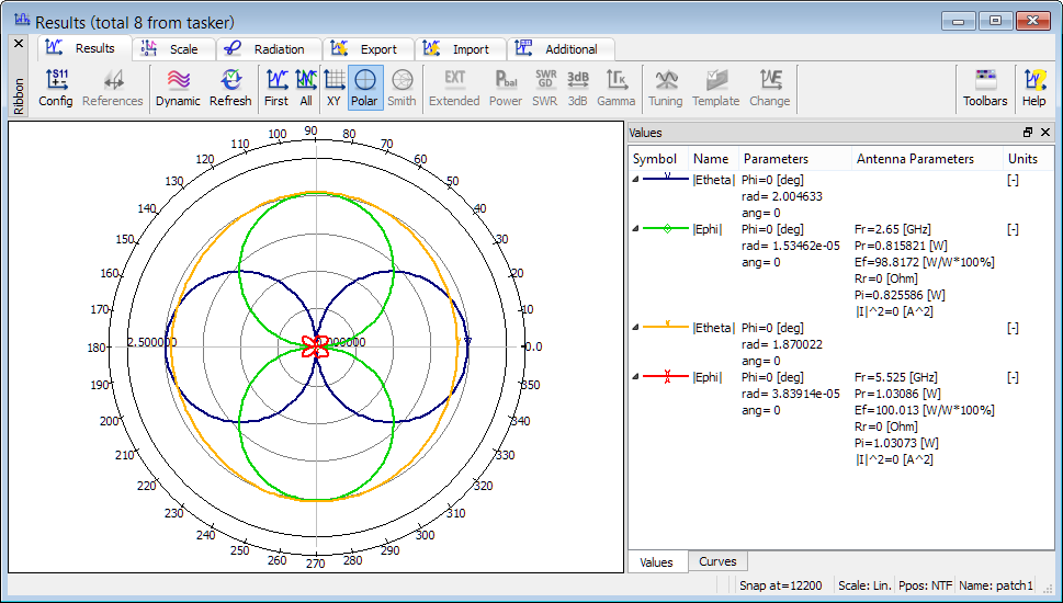
Fig. 2.3.3-4 Radiation patterns versus azimuthal angle Phi with elevation angle Theta=30° calculated in the example patch1.pro for two frequencies: 2.65 and 5.525 GHz.
Let us now calculate the radiation patterns versus azimuthal angle (Phi) with Theta=30°. The results are presented in Fig. 2.3.3-4 in polar coordinates and can be displayed by pressing ![]() button in 2D Radiation Pattern section of Results tab of QW-Simulator. Let us note that together with radiation patterns the software displays antenna efficiency which indicates (in percents) the ratio of the power radiated by the antenna (calculated at the NTF box) to the power injected into the antenna by the source. We are exciting the structure with a pulse of limited duration and thus after sufficiently long FDTD simulation of a lossless antenna the efficiency should reach 100%. As seen in Fig. 2.3.3-3 this is the case at 5.525 GHz. At 2.65 GHz the efficiency is 98.8 %. This indicates that the resonance at 2.65 GHz has a higher Q-factor and thus after 12200 iteration there is still some energy at this frequency accumulated inside the NTF box.
button in 2D Radiation Pattern section of Results tab of QW-Simulator. Let us note that together with radiation patterns the software displays antenna efficiency which indicates (in percents) the ratio of the power radiated by the antenna (calculated at the NTF box) to the power injected into the antenna by the source. We are exciting the structure with a pulse of limited duration and thus after sufficiently long FDTD simulation of a lossless antenna the efficiency should reach 100%. As seen in Fig. 2.3.3-3 this is the case at 5.525 GHz. At 2.65 GHz the efficiency is 98.8 %. This indicates that the resonance at 2.65 GHz has a higher Q-factor and thus after 12200 iteration there is still some energy at this frequency accumulated inside the NTF box.
Note that antenna efficiency is a valuable measure of convergence of QW-3D simulations in the case of lossless antennas, just like power balance in the case of lossless circuits. Moreover, if losses are subsequently included in the analysis, we can expect that the simulations will converge faster than in the corresponding lossless case.
In practical designs it often happens that a patch antenna is fed with a vertical coaxial line. Such a line may have a very small diameter, when compared to the dimensions of the patch and to the considered wavelengths. In such a case it would be impractical to mesh the cross-section of the line into sufficiently small FDTD cells reproducing accurately the cylindrical shape of the conductors. This would unnecessarily provoke a drastic increase in the overall computing time of the project.
Thus in patch1.pro we use a different approach. We approximate the cross-section of the dielectric filling of the coax by a rectangular shape composed of four FDTD cells. In the centre we place a wire. The diameter of the wire is chosen so that the characteristic impedance of the line adopts the desired value (in our case 50 W). Please look at the right hand side of Fig. 2.3.3-1 where we present a fragment of the FDTD mesh around the feeding line. The basic mesh resolution is 3 mm. The dielectric cross-section is marked as a blue square 2 x 2 mm. Moreover, we have set the thickness of the outer conductor of the line at 1 mm and put the mesh snapping planes along all its sides. The metal outer circumference is shown in brown, and the mesh snapping planes – in green. We have obtained a local mesh refinement (3 x 3 cells) in a sensitive area of the feeding point. Inside the patch1.udo script the wire diameter is set to cxd/exp(cimp/60) where cxd is the diameter of the coax (2 mm) and cimp is its desired characteristic impedance (50 W). This arrangement produces a very good approximation of a 50 W feeding coax line.
The above approximation of a thin coax line is not the only possible one. In patch2.pro (using patch2.udo) we apply a different one. Instead of connecting the coax line, we put a lumped source between the patch and the ground plane. Let us note however that a lumped source extends over one FDTD cell. Thus if the antenna dielectric substrate is modelled by more than one layer of the FDTD cells, we should extend the lumped source by a thin wire, so that the current can flow between the patch and the ground. The library object patch2.udo generates such a lumped source and if needed extends it by a wire. We suggest that the readers interested more deeply in application of UDO language have a look into the patch2.udo script to see how this is achieved with available UDO commands.
It is interesting to run the simulation of patch2.pro and compare the results with patch1.pro. The differences are insignificant and thus we can conclude that both approximations of a thin coax line: by a 4-cells square line and by a lumped source give similarly good accuracy.
It may be also interesting to have a look at the project patch3.pro. It also uses patch2.udo but instead of ..\boxes\ntf.udo it uses ..\boxes\pmlntf.udo. Thus instead of superabsorbing boundary a Perfectly Matched Layer (PML) is applied. Comparison of the results obtained with patch2.pro and patch3.pro indicates insignificant differences between them and brings the conclusion that both types of absorbing boundaries are applicable here.
Fig. 2.3.3-5 shows the parameters of the bottom PML wall. What we need to select first is the conductivity profile, set as Parabolic in this example (and in most usual applications). It means that PML conductivity varies as: A*x^2, where x=(distance from PML edge)/(PML thickness).
The other possibility, not used in this example but shown in the lower part of the figure, is Exponential profile. Its conductivity varies as: A*exp(B*x) with x defined as above, and A, B set in the dialogue.
However, let us note an important geometrical restriction on superabsorbing and PML boundary application in a general case. Both types of absorbing boundaries penetrate from the plane where they are formally defined into the meshed area. Superabsorbing boundary penetrates only two FDTD cells inside. This means that the NTF box must be placed not less than 3 FDTD cells from the superabsorbing plane. For the PML boundary we declare its thickness in Add ABC Wall/Edit ABC Wall dialogue. Typical thickness is 4-8 cells and thus the margin where we cannot place the NTF box becomes significantly wider. Note that in XY plane displays of QW-Editor the mesh lines show only the boundaries between entire FDTD cells while in XZ and YZ plane also half-cell levels are indicated. This should be taken into account to avoid confusion when calculating the distance (in cells) from an element to an absorbing boundary.
Let us also note that the above formal restriction on placing the elements far away from the absorbing boundary is not the only one. We should also be aware that the absorbing boundaries of both types should be placed at sufficient distance from the radiating element so that the radiation fields dominate there. When the absorbing boundary is placed in the area of high density of the close (inductive) fields of the antenna, it can significantly change its radiation patterns. The minimum distance depends on application but typically at least half-wavelength is recommended.
When comparing the available absorbing boundaries, we should remember about one more important restriction on the PML. It must extend over the entire side of the meshed area and cannot interact with other elements except for other PML walls. Otherwise the FDTD algorithm instability may occur. This practically limits the application of PML to the absorbing box used in antenna analysis while superabsorbing boundary can also be used also for a variety of other applications like surrounding and terminating transmission lines.
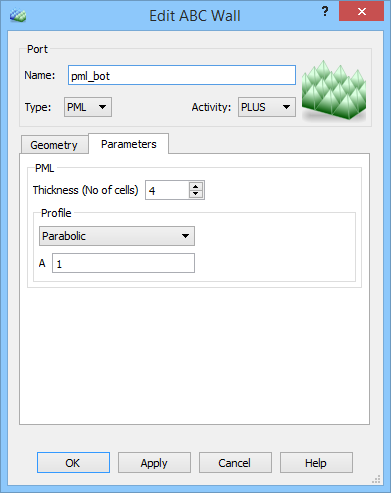
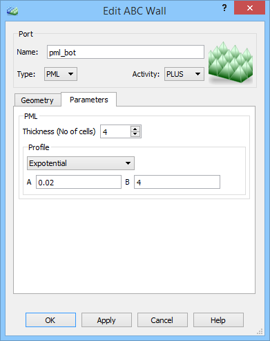
Fig. 2.3.3-5 Edit ABC Wall dialogue for a PML absorbing wall.