2.2.9 Planar circuit
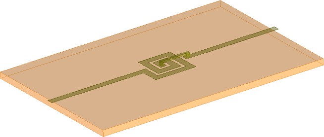
Here we will consider simulation of a planar inductor as presented in Fig. 2.2.9-1.The structure has been originally designed and measured by Becks and Wolff in “Analysis of 3-D metallization structures by a full-wave spectral domain technique”, IEEE Trans. Microwave Theory Tech., vol. MTT-40, No.12, Dec.1992, pp.2219-2227. It has been prepared for QW-3D simulation and stored in the file: ..\PassiveComponents\Planar\induct1.pro.
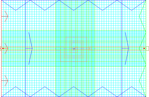
Fig. 2.2.9-1 Planar inductor and its presentation in the 2D window of QW-Editor.
The project is composed of 7 objects called from standard QW-3D libraries. Please invoke Select Object dialogue to see the list of these objects (marked as UDO objects). They are:
msps - describing the microstrip substrate and upper absorption (generated by a call to ..\planar\msps.udo);
bbox - describing the two side absorbing walls (generated by a call to ..\boxes\bbox.udo);
inpp, outp - describing the input and output ports (generated by calls to ..\ports\ portoye.udo);
msi1sp - describing the spiral (generated by a call to ..\planarsp\msi1sp.udo);
outl - describing the output segment of microstrip line (generated by a call to ..\planar\ msl.udo);
msb - describing the air bridge (generated by a call to ..\planar\msb.udo).
Please double click over each of them to see the actual values of parameters used for the project. The above objects describe the entire structure to be analysed. However on the list of elements (seen in Select Element dialogue) we can find some, which have not been not generated by any of the objects. These are the mesh snapping planes of electric type (enforcing in the particular plane the edge of FDTD cells so that the tangential electric field is defined there). They are named electric2...electric10. In the project there are also some other mesh snapping planes named sp... which have been generated from the objects. All of them play an important role in assuring optimum meshing of the structure. First of all, they are used to adjust the FDTD grid so that the edges of strips coincide with the edges of the rows of FDTD cells. In such a case QW-3D can recognize the edge and apply automatically special models of field singularities. These models decisively increase the accuracy of the analysis of planar structures, especially in terms of characteristic impedance of the strips. When applied, they produce good approximation of the characteristic impedance of the strip even with 2-3 FDTD cells across the strip width. Without them similar accuracy can be obtained with 7-8 FDTD cells per strip width. That is why it is recommended that the mesh snapping planes of electric type be placed along the strip edges.
![]()
![]()
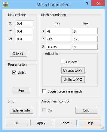
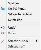
Fig. 2.2.9-2 Line change menu.![]()
![]() Fig. 2.2.9-3 Mesh parameters menu.
Fig. 2.2.9-3 Mesh parameters menu.
In some of the library objects these planes are generated automatically (e.g. msi1sp.udo). But sometimes they need to be supplemented by the user. As examples we can quote here electric7...electric10 used to snap the mesh to the side of the air bridge and to the edge of the output line. Let us run an exercise of introducing mesh snapping planes adjusted to an edge of a particular element. We start by deleting from the list of elements electric7..electric8. We can see that the light-green lines along the air bridge have vanished. Now we invoke again the list of elements and double click over msbcl that describes the bridge. We return to the 2D Window. We can see that the cursor has changed to a square one indicating that we are in the Edit mode. Now let us choose Edit Line and click (only once!) over an edge of the bridge. To be sure that we have chosen the right edge we can drag it a little. Now please press the right mouse button to see the window as in Fig. 2.2.9-2. Pressing over Set electric splane will produce the mesh snapping planes along the chosen line. The line dragged from its original position should return to it. We can see that the mesh has been snapped to the edge and the newly generated mesh snapping plane has appeared on the list of elements. Now we can choose another line and proceed like before.
When finished, we should press Selection off in the window of Fig. 2.2.9-2or keyboard E to escape from the Edit mode of the cursor. The cursor should return to its original arrow shape. If we fail to do it before moving to other windows, we can experience unpleasant effects of not being able to access one window hidden under another one.
There is also another important application of the mesh snapping planes. They can be used to define an area of different mesh refinement. In the considered project electric2..electric6 have been used for this purpose. They do not need to be adjusted to the particular edge of an element and thus the best way of generating them is through Special Planes and Boundaries dialogue. We can choose Force mesh: Electric and then choose the particular Orientation and Position. Clicking over Insert will generate the desired mesh snapping plane. If we want to use such a plane to enforce the particular cell size up or down from it, we should proceed as follows. We invoke the Select Element dialogue and double click over the name of the chosen mesh snapping plane. Now we press the right mouse button over the 2D Window and choose Edit command to open the Edit Special Plane, Boundary... dialogue. In its lower part we can chose the size of the Forced cell size up from the plane (plus) or down from the plane (minus).
Let us now have a closer look at the ports in the original ..\PassiveComponents\Planar\induct1.pro project. We invoke Transmission Line Ports dialogue and see that we have two ports. After invoking ABCsdialogue we see that there are three absorbing walls, for which the only parameter to be considered is the effective permittivity. Its choice has some influence on the parameters of superabsorbing boundary and thus should be close to real effective permittivity for the plane propagating close to the boundary. In the considered project we have chosen it to be equal 1 for the upper absorbing wall and 6.5 for the side absorbing walls partly adjacent to the dielectric substrate.
Now let us look at the two transmission line ports: inpp and outp in corresponding Edit Transmission Line Port dialogues. Both have been declared with Exciting field: TEM. This means that the software will calculate a mode template based on quasi-static solution of the field distribution in the port cross section. It will start calculation of this solution from finding the first conductor. QW-Editor indicates excitation point for each port. This point can be seen in the QW-Editor 2D Windows (as a red cross or segment). It can be moved by choosing the particular port (for example Input Template [1]) on the list of elements and pressing over Select P(lane) and later Edit Point. For a TEM port the excitation point indicates where the software should look for the first conductor. During the TEM template generation it assigns unitary potential to this conductor and zero potential to all the other conductors. If the declared excitation point is outside metal, the software issues a warning and tries to find the first conductor itself. In the considered project the excitation points in both inpp and outp are placed on the strips of the input/output lines.
To continue tutorial comments on the..\PassiveComponents\Planar\induct1.pro let us note that the input/output strips slightly extend over the meshed area. Normally the software meshes the entire area including all the elements. However, this can be changed in Mesh Parameters dialogue by unchecking the box Adjust to Objects as seen in Fig. 2.2.9-3. Mesh boundaries can be then set as needed. In this project such an option has been applied.
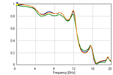
Fig. 2.2.9-4 |S21| calculated with induct1.pro (red curve), with induct2.pro (blue curve) and measured by Becks and Wolff (green curve).
Now let us run the simulation of ..\PassiveComponents\Planar\induct1.pro. First let us look at the Simulator Log of QW-Simulator. In its upper part we can see that the software has calculated the quasi-static (TEM) templates for input/output ports and displayed for both of them the characteristic impedance of the line Zo=49.2981 and effective permittivity Eef=6.4824. After about 12000 iterations of the 3D simulation the results of S-parameters are ready to be investigated. Fig. 2.2.9-4presents the results of Abs(S21) calculated with induct1.pro (red curve) and measured by Becks and Wolff (green curve). The agreement is very good. In the range up to 10 GHz the measured values are lower than simulated values by about 0.2 dB. A similar effect has been detected by Becks and Wolff and thus we can assume that they are due to technological uncertainties.
So far we have calculated our inductor example assuming quasi-static templates in the input/output lines. However, it is well known that at higher frequencies the field distribution in a microstrip line can be significantly different than its quasi-static approximation. The wave is not purely TEM, its characteristic impedance becomes difficult to define and the effective permittivity varies with frequency. We can expect that this may be the case in the upper frequency band of our example. Thus we can suspect that in that band the difference between the real and assumed template can to some extend influence the results of the analysis. To verify this, let us now consider induct2.pro, which is prepared to calculate the same problem as induct1.pro but assuming the mode template in microstrip line for 18 GHz. At this frequency we cannot assume that the field distribution is the same as in TEM line and we must calculate the mode template using the same mechanism as previously used in calculating templates for waveguide modes (see sections from Septum polariserto Modal templates in inhomogeneous guides).
In induct2.pro let us open Edit Transmission Line Port dialogue for the input port (see Fig. 2.2.9-5). We can see that the type of Exciting field has been changed to Arbitrary. The correct setting of effective permittivity is now crucial for generating the needed mode at the needed frequency (see the explanations in First insight template generation). In this example it is set to 7.3. We are expecting to find the mode close to 18 GHz and we are searching for it in the 17 to 19 GHz band.
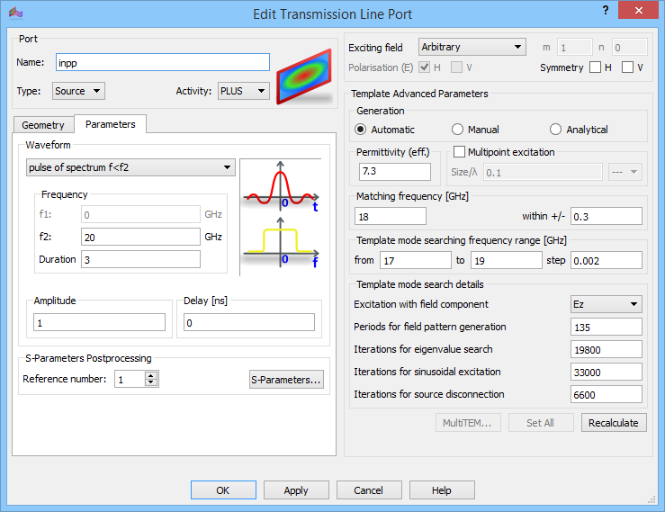
Fig. 2.2.9-5 Edit Transmission Line Port dialogue for the input port of induct2.pro.
Let us now run induct2.pro. First we look at the Simulator Log in the part where the template generation is described. It proceeds the same way as in the case of waveguide mode templates generation (see First insight template generation). We can note that our guess of effective permittivity equal to 7.3 has been correct since the mode has been found very close to 18 GHz. Let us also note that (contrary to the case of TEM template) the software does not show the value of the characteristic impedance of the input line. This is due to the fact that in the case of Arbitrary mode the wave in the line is not purely TEM and thus the notions of voltage, current and impedance cannot be uniquely defined.
Now we run the 3D simulations of induct2.pro for about 12000 iterations. In Fig. 2.2.9-4the obtained results (blue and green curves) are compared with the results previously obtained using TEM templates in induct1.pro (yellow and red curves). The differences are practically insignificant, which indicates good wide-band properties of the QW-3D system of S-parameter extraction working well even with templates varying with frequency. Let us however note that in the considered example the error generated by frequency varying field distribution of the template might have been partially cancelled because the input and output lines are the same. Such errors may be somewhat more pronounced with different geometries of the input and output lines. Thus in case of doubts as to the possible influence of the template variation with frequency it is recommended to run the calculation twice: with template from the lower and upper part of the considered band. We can treat the comparison of the results of calculation with induct1.pro and induct2.pro as an example of application of such a procedure.
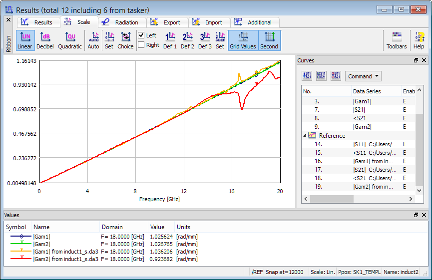
Fig. 2.2.9-6 Propagation constants versus frequency calculated with induct1.pro and induct2.pro.
It is worth noting that the results obtained with QW-3D can be used to obtain the dispersion characteristics of the input/output lines. Fig. 2.2.9-6presents the propagation constants at the input and output lines calculated with induct1.pro (yellow and red curves) and induct2.pro (blue and green curves). As the first comment let us note that induct1.pro results seem accurate only to about 10 GHz while induct2.pro results are correct in the entire band. In induct1.pro we use the TEM templates, which are not accurate at higher frequencies. The templates are used to filter the desired mode in the input/output line from other modes, which may appear in these lines close to discontinuities. With TEM templates used above 10 GHz the software cannot precisely separate the dominant mode from higher modes and thus an error in extraction of the propagation constant appears. Similar errors do not appear when we use high frequency templates for S-parameter extraction at lower frequencies because the amplitudes of higher modes are smaller at low frequencies. This explains correct results obtained with induct2.pro in the entire band.
The results as those presented in Fig. 2.2.9-6can be used to extract changes of the effective permittivity of the microstrip line versus frequency. For example we can see that for 18 GHz b = 1.026 [1/mm]= sqrt(eef )w/c. Thus we can calculate eef = 7.4. This value is slightly higher than the value of 7.3 used successfully for extracting the mode template at this frequency. The difference is due to the effect of dispersion of the 3D FDTD algorithm with a relatively coarse mesh of 0.4 mm along the port lines in induct2.pro. It can be verified that reducing the cell size in y-direction to 0.2 mm eliminates most of this error and brings the value of the effective permittivity at 18 GHz (extracted from 3D simulations) very close to 7.3.