your partner in EM modelling & research
- Home
- EM Software
- ACADEMIC
-
Applications
-
Area of Applications
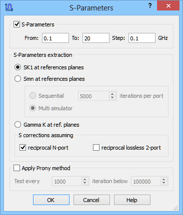
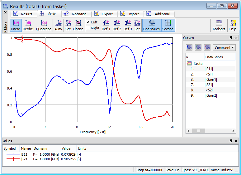
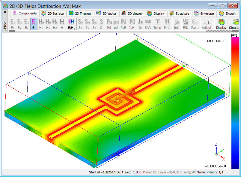
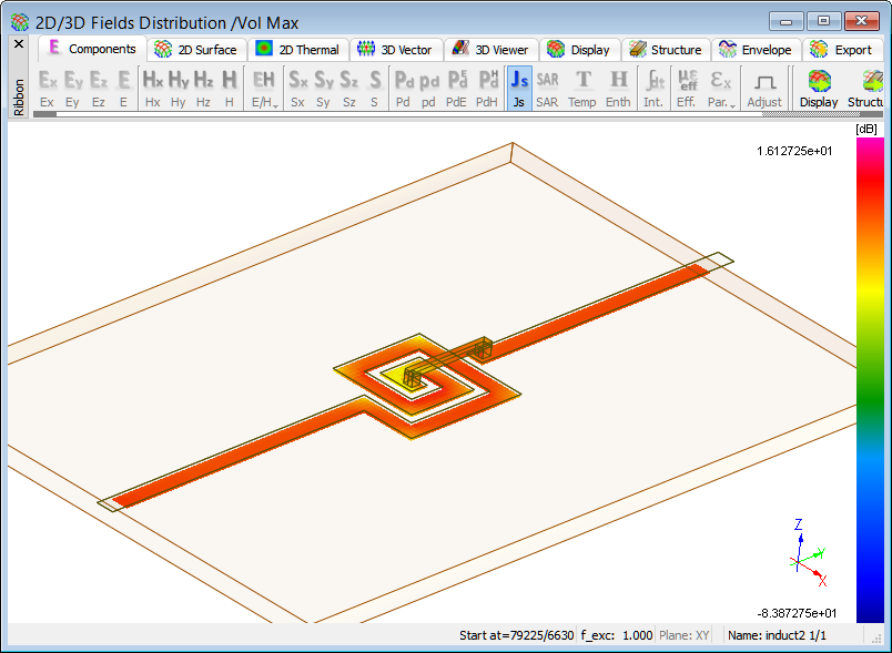
- S-Parameters Extraction
- Radiation and Scattering Problems
- Microwave Heating
- Bodies of Revolution (V2D)
- Materials
- Waveguides
- Planar Structures
- Resonators
- Filters
- Periodic Structures
- Free Space Incident Wave
- Frequency Domain Monitoring
- Photonic Crystals
- High Q Structures
- Optimisation
- Time Domain Reflectometry
- Field Integration Along Contours
- White Papers
- Co-Processings
- Post-Processings
-
Area of Applications
- Measurement Setups
- Services
- Users
- Elsevier MW Book