NanoBat
GHz nanoscale electrical and dielectric measurements
of the solid-electrolyte interphase
and applications in the battery manufacturing line
Coplanar Waveguide Examples: a popular GHz transmission line finding use in material measurements
Download CPW examples (ZIP file).
Note: if the link does not open automatically, press right mouse button, choose �Copy link address� and paste it into a new browser window.
What is a Coplanar Waveguide?
Coplanar waveguides (CPW) are a well-known type of transmission lines, used for example, to transmit electrical signals in the microwave and millimeter-wave range. CPWs take the form of three parallel metallic strips placed on a dielectric substrate, where the central strip is the "hot" conductor and two (broader) strips serve as a ground plane. This geometry makes CPW convenient for use in planar circuits, as connecting lumped elements between the hot conductor and the ground plane does not require making holes and vias in the substrate. CPWs are therefore traditionally used as elements of integrated circuits (ICs). A less traditional application of CPWs is the construction of measurement probes (or sensors) for investigating the electromagnetic properties of unknown volumetric samples, in particular for measuring complex permittivity. Both kinds of applications are illustrated with the provided examples.
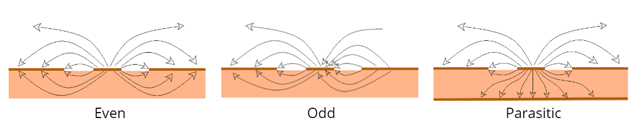
A CPW is a multimodal transmission line of quasi-TEM type. From the mathematical properties of the Laplace equation we know that a TEM line comprising N independent conductors supports (N-1) modes of EM energy propagation. Hence in its generic configuration of three conductors, a CPW supports two modes: even and odd. In a more practical configuration with an additional common ground plane below the substrate, there is also a third mode, sometimes called "parasitic microstrip mode". In most applications, the even mode is the desired one, but the other modes are generated at waveguide bends and other discontinuities, inevitable in a real circuit.
Knowing the properties of all three modes � their field patterns, propagation constants, model impedances � is important for designing CPW circuits for any application.
Examples illustrating CPW modes, their coupling, and coupling suppression
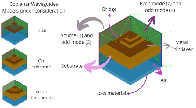
The provided set of examples includes two CPW topologies:
- a straight uniform section of CPW, without discontinuities,
- a 90deg CPW bend.
Both topologies are considered as "suspended in air" or placed on a dielectric substrate. The first case is idealistic (though approximates a CPW on ultra-low-permittivity substrate) and serves to demonstrate pure TEM modes in a multi-conductor transmission line. In particular, we see that the three modes have different cross-sectional EM field patterns (corresponding to the generic pictures above) but identical phase velocities and propagation constants. In the presence of the substrate, the different field patterns lead to different propagation constants, as there is a different split of EM energy into the substrate and the air medium.
In a straight CPW section (without longitudinal discontinuities) there is no coupling between the modes. Hence if a pure even mode is ideally excited, we expect no transmission into the odd mode. In the simulation, residual levels of such cross-talk are observed, since the modal pattern (and also the effective permittivity) slightly vary with frequency, while the numerical generation of the mode (and then its filtering for S-parameter extraction) are performed with a constant cross-sectional field template.
The most interesting example is the CPW bend. Here, the discontinuity causes the coupling of EM energy from the excited even mode into the odd mode. This is demonstrated by the figure below, where port (1) is assigned to the source (even mode at input), port (2) is the even mode at output, while ports (3) and (4) are assigned to the odd mode at the input and output planes, respectively.
Additional examples illustrates two popular ways of supersign the modal coupling, by a bridge (connecting the two strips meant to serve as a ground) and by a miter of the bend.
Examples illustrating CPW application in material measurements
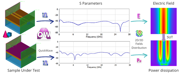
The previous examples have already shown that properties of a CPW, such as its modal impedances and propagation constants, change in response to the permittivity of the substrate. By analogy, we may now consider placing a dielectric slab over the CPW. Thereby, a portion of energy that would normally propagate in air is forced to propagate in the slab (being our sample-under-test, SUT); the phase velocity will change and so will the modal impedances and propagation constants. We may detect and measure such changes in order to characterise the SUT properties. The use of CPW for material measurements is appealing since:
- the measurement is simple and non-destructive,
- we expect low sensitivity of the results to geometric dimensions of the sample.
We may envisage:
- covering the full length of the CPW with the SUT and measuring changes in propagation constant (phase of S21 indicating the real and amplitude- the imaginary part of complex permittivity),
- covering a section of the CPW with the SUT and measuring S11 and S21.
The second setup is more practical but both are illustrated with the provided modelling examples. In both setups, modelling is necessary for converting the measured result into the SUT properties.
The NanoBat project has received funding from the European Union's Horizon 2020 research and innovation programme under grant agreement No 861962.