2.2.7 Dielectric waveguide coupler
Let us consider the analysis of a dielectric waveguide 3-dB coupler. Its general view is presented in Fig. 2.2.7-1. Since some of the readers may not be familiar with the principle of its operation we will first provide some brief explanation in this regard. The coupler is composed of a cross-junction of dielectric waveguides. In general it may be shielded or unshielded. In the considered case we assume that the box is unshielded above and that there is an electric plane at the bottom of the structure of Fig. 2.2.7-1. This kind of a model can correspond to two physical situations: one in which a metal plate supports dielectrics (image waveguide case) and the second in which there is no horizontal metal plate but the electric plane of the model (presented in Fig. 2.2.7-1) corresponds to the symmetry plane of the structure (rectangular dielectric waveguide case). The cross-junction is made of a dielectric of a relatively low permittivity (er=2.55 in the considered example). The centre of the junction is cut by a plate inclined at 45° made of a dielectric of higher permittivity (er=7.0 in the considered example) that serves as a semi-transparent mirror. The coupler is excited by the dominant dielectric waveguide mode from the left. Assuming its ideal operation we should have half of the power transmitted straight to the right port and half of the power reflected by the plate to the upper port. There should be no power transmission to the lower port.
Fig. 2.2.7-1 A general view of the dielectric waveguide 3-dB coupler considered in the example ..\PassiveComponents\Dcoupler\dcoup1.pro.
The coupler project has been stored in the file ..\PassiveComponents\Dcoupler\dcoup1.pro. It has been prepared using ..\examples\dcoup1.udo. This UDO allows changing various parameters of the coupler, for example dimensions of the box, the dielectric waveguide and the plate as well as the kind of dielectric materials used for the dielectric waveguide and the plate. The default parameters used in dcoup1.udo have been chosen for the best performance of the coupler at about 95-100 GHz.
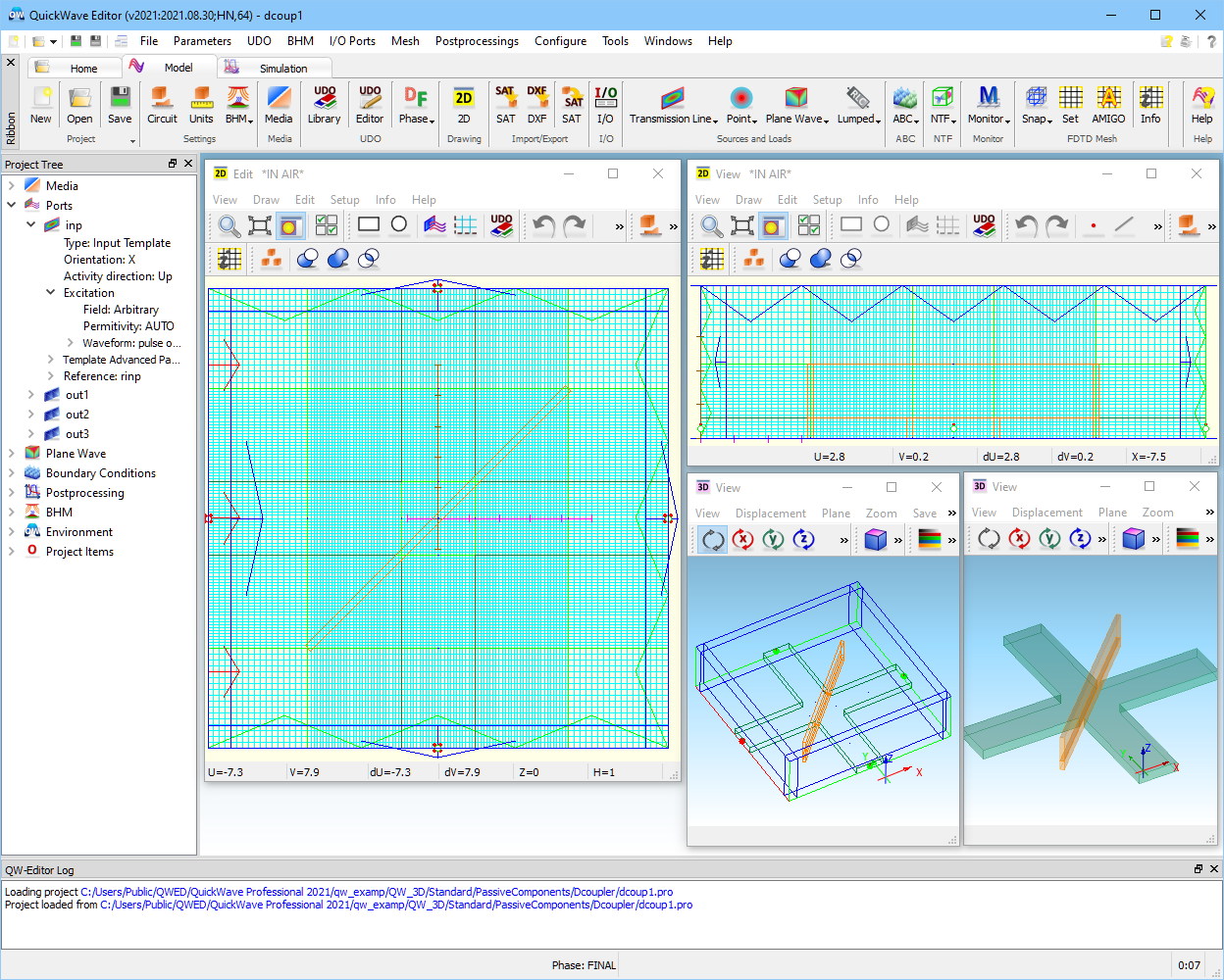
A look at the structure presented in 2Dand 3D Windows of QW-Editor for the loaded project as well as on the list of elements in Select Element dialogue confirms that four ports have been defined. Each of the ports extends over one side of the square box and thus they have the same size. Moreover, all of them have been defined for the dominant mode of the dielectric waveguide. Thus their parameters can be stored in the same port parameters file dielp.iop. Having dcoup1.pro open in QW-Editor, we press ![]() button and QW-Simulator starts its run from calculating the mode templates at the dielectric waveguide ports. Let us wait until the Simulator Log displays the sequence of messages:
button and QW-Simulator starts its run from calculating the mode templates at the dielectric waveguide ports. Let us wait until the Simulator Log displays the sequence of messages:

and then press ![]() button from 2D/3D Fields tab to see the template field distribution as presented in Fig. 2.2.7-2. As expected for this kind of waveguide, vertical electric fields dominate and it is confined to the region of the dielectric. It is interesting to note a visible discontinuity of this field at the top of the dielectric surface enforced by the boundary condition imposing continuity of the displacement vector.
button from 2D/3D Fields tab to see the template field distribution as presented in Fig. 2.2.7-2. As expected for this kind of waveguide, vertical electric fields dominate and it is confined to the region of the dielectric. It is interesting to note a visible discontinuity of this field at the top of the dielectric surface enforced by the boundary condition imposing continuity of the displacement vector.
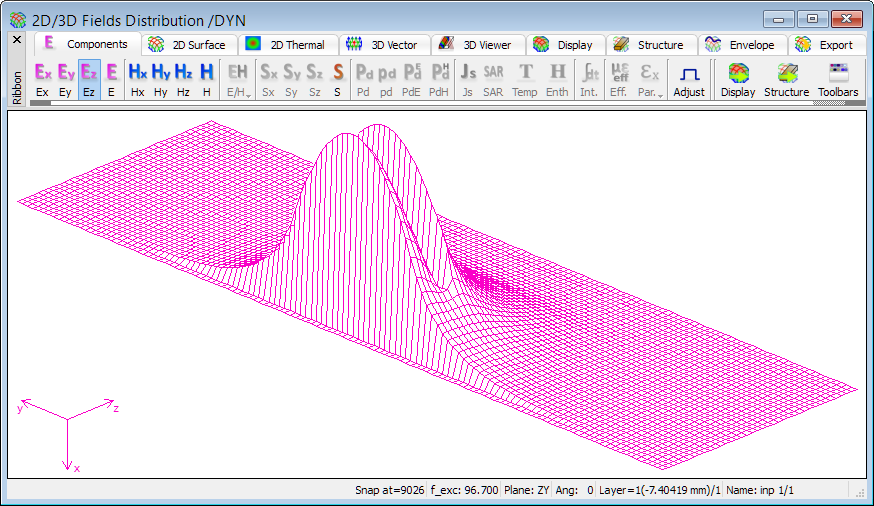
Fig. 2.2.7-2 Ez filed distribution across a dielectric waveguide port of dcoup1.pro.
Let us now continue the simulation of the example. After calculating the mode templates for all four ports the software starts the 3D analysis. At this stage it is interesting to press ![]() button once again; the proper FDTD mesh level allowing watching how the pulse propagates across the coupler is already set (to switch between the consecutive FDTD mesh levels use K or L at the keyboard). Please press also
button once again; the proper FDTD mesh level allowing watching how the pulse propagates across the coupler is already set (to switch between the consecutive FDTD mesh levels use K or L at the keyboard). Please press also ![]() button in Resultstab to open Resultswindow to see how the S-parameters versus frequency are calculated. Refresh Settings has been set to 50 FDTD iterations to enable tracking the convergence of the S-parameter curves to their final shape. After about 1500 iterations we can see the final results as presented in Fig. 2.2.7-3. As expected, the transmissions to port 2 and port 3 are almost equal in a wide frequency band from 80 to 110 GHz. However, the level of |S21| and |S31| is about 1.3 dB lower than the expected –3 dB. This difference cannot be explained by the input reflection and transmission to port 4 that are both very low. Thus some of the energy must be transferred to modes different than the dominant one and/or dissipated at the top absorbing boundary (simulating physical conditions of the free space).
button in Resultstab to open Resultswindow to see how the S-parameters versus frequency are calculated. Refresh Settings has been set to 50 FDTD iterations to enable tracking the convergence of the S-parameter curves to their final shape. After about 1500 iterations we can see the final results as presented in Fig. 2.2.7-3. As expected, the transmissions to port 2 and port 3 are almost equal in a wide frequency band from 80 to 110 GHz. However, the level of |S21| and |S31| is about 1.3 dB lower than the expected –3 dB. This difference cannot be explained by the input reflection and transmission to port 4 that are both very low. Thus some of the energy must be transferred to modes different than the dominant one and/or dissipated at the top absorbing boundary (simulating physical conditions of the free space).
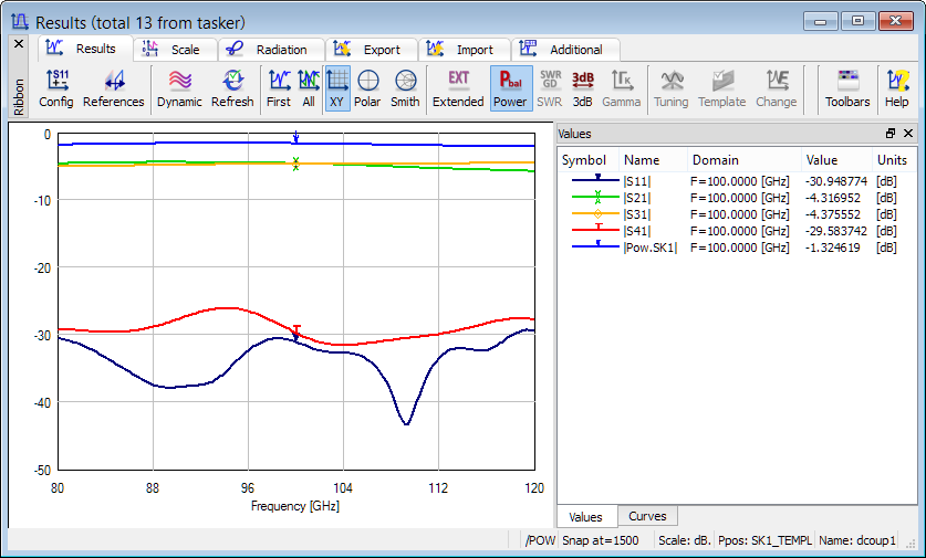
Fig. 2.2.7-3 Results of analysis of S-parameters of dcoup1.pro in 80-120 GHz band.

Fig. 2.2.7-4 Envelope maximum of Ez field of dcoup1.pro at 95 GHz.
It is also interesting to re-run the dcoup1.pro example after changing in QW-Editor in Edit Transmission Line Port dialogue the Excitation waveform of the source port to sinusoidal with f1=95 GHz. After achieving the steady state of the simulations press ![]() button, the field component Ez is already chosen, press D over the image to get the dynamic refreshment of the field display window and press E at the keyboard to get into Envelope Maximum mode of operation. You will obtain the picture as shown in Fig. 2.2.7-4. We can see how the input wave is separated into two waves of smaller amplitudes. We can also see that some of the fields are scattered into diagonal directions of the box. This justifies some losses of energy that were detected in the S-parameter calculations.
button, the field component Ez is already chosen, press D over the image to get the dynamic refreshment of the field display window and press E at the keyboard to get into Envelope Maximum mode of operation. You will obtain the picture as shown in Fig. 2.2.7-4. We can see how the input wave is separated into two waves of smaller amplitudes. We can also see that some of the fields are scattered into diagonal directions of the box. This justifies some losses of energy that were detected in the S-parameter calculations.