2.17.1 Plane wave excitation
Consider the excitation of the electromagnetic plane wave (PLW). In Plane wave excitation and scattering we have already introduced the plane wave excitation inside the limited volume with the PLW box. However, in some applications it is desirable to analyze plane wave illumination of the infinitely periodic structure. Such problems occur in optics where diffraction gratings as well as the other kinds of frequency selective surfaces are growing interest. Direct FDTD modelling of the infinite periodic structure is impossible because of the finite computer resources. Approximation of the infinite problem by using a large number of the grating periods is possible but inefficient.
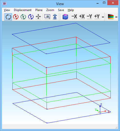
Fig. 2.17.1-1 3D view of the scattering1.pro model.
Periodic boundary conditions implemented in QW-3D software package allows reducing the model size to only one period of the structure.

Fig. 2.17.1-2 Circuit dialogue.
Open the example ...Scattering\Periodic\scattering1.pro. First, we will try to excite the plane wave without the scattering body to understand the principles of the periodic boundary conditions (PBC). In a 3D Window (see Fig. 2.17.1-1) we may see that indeed there is no scattering body in the scenario. Red colour indicates plane wave walls, whereas green one indicates NTF walls. We impose PBC along X and Y assuming infinite extension in these directions. As a consequence, both PLW and NTF boxes stick to the lateral boundaries of the scenario.
Invoke Circuit dialogue (![]() button in Model tab of QW-Editor). The type of the circuit is set to 3DP with periodicity in X and Y direction. It means that periodic boundary conditions are located at the lateral boundaries of the scenario and force a particular Floquet Phase shift per period set in Circuit dialogue (see Fig. 2.17.1-2).
button in Model tab of QW-Editor). The type of the circuit is set to 3DP with periodicity in X and Y direction. It means that periodic boundary conditions are located at the lateral boundaries of the scenario and force a particular Floquet Phase shift per period set in Circuit dialogue (see Fig. 2.17.1-2).
Excite TE polarised plane wave in (φ, θ) = (0, 135) direction, where φ, θ are the spherical coordinates with the Z reference axis. In such a case, Floquet phase shift per period ψ may be easily calculated from the following relations:
![]()
![]()
![]()
(2.17.1-1)
where Li is a spatial period of the structure along i axis and c stands for the light velocity. Since we impose periodicity only along X and Y directions, phase shift ψz is not needed. According to eq. (2.17.1-1) the angle of incidence is frequency dependent if the phase shift per period ψ is fixed. In other words, pulse excitation in PLW box may generate a set of plane waves with a variable angle of incidence. However, if a relatively narrow excitation bandwidth is set we may assume that deviation of the angle of incidence may be neglected.
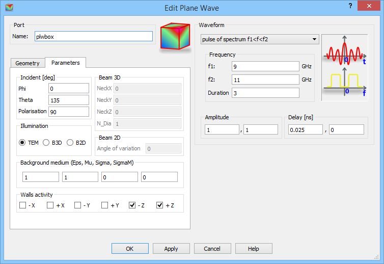
Fig. 2.17.1-3 Edit Plane Wave dialogue.
Invoke Edit Plane Wave dialogue (see Fig. 2.17.1-3). The excitation spectrum is around 10 GHz. The plane wave illumination angle indeed has been set to (φ, θ) = (00, 1350). However, since we have set PBC along x and y directions, only Z-directed walls of the PLW box will be used for exciting the wave. The four X and Y walls are deactivated in the Active walls frame.
According to the fundamentals of the periodic FDTD algorithm described in [17] and implemented in QW-3D, real and imaginary grids of electromagnetic components are defined. Calculation of both grids is performed independently except for the periodic boundaries where these grids are coupled according to the phase coefficient ej. In our example, amplitude has been set to both real and imaginary grids (see Fig. 2.17.1-3). Moreover, in order to excite a pure travelling plane wave, excitation delay between the two grids has to be set to the quarter of the period (quadrature) at the frequency of our interest, i.e. 10 GHz. In this case delay of the imaginary grid excitation amounts to 0.025 ns.

Fig. 2.17.1-4 Pickup Walls dialogue of QW‑Simulator in scattering1.pro example.
Run the simulation using ![]() button from Simulation tab of QW-Editor. After simulation converges open Results window with scattering pattern in the XZ-plane by pressing
button from Simulation tab of QW-Editor. After simulation converges open Results window with scattering pattern in the XZ-plane by pressing ![]() button in Results tab of QW-Simulator. By pressing the NTF Walls button of the Radiation Patterns dialogue, we obtain the Pickup Walls dialogue of Fig. 2.17.1-4. It shows that only one wall of the NTF box will take part in NTF calculations. This is +Z wall located just below the active PLW wall, and flux of power is incoming through this wall. Therefore the value of radiated (outgoing) power shown in the window status of Fig. 2.17.1-5 is negative: Pr=-5968.4648 [W].
button in Results tab of QW-Simulator. By pressing the NTF Walls button of the Radiation Patterns dialogue, we obtain the Pickup Walls dialogue of Fig. 2.17.1-4. It shows that only one wall of the NTF box will take part in NTF calculations. This is +Z wall located just below the active PLW wall, and flux of power is incoming through this wall. Therefore the value of radiated (outgoing) power shown in the window status of Fig. 2.17.1-5 is negative: Pr=-5968.4648 [W].
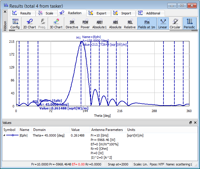
Fig. 2.17.1-5 Results window with scattering pattern for the scattering1 example.
There is an incident lobe indicated around θ = 1350 (see Fig. 2.17.1-5, which is consistent with the settings of Theta in the Plane Wave dialogue. Since there is no scattering body inside the considered volume we observe nulls at all of the possible diffraction orders indicated with the vertical dashed lines (![]() button in Results window). Due to the finite size of NTF wall, where the Fourier transform is performed, radiation pattern is somewhat broadened, rather than the Dirac delta. Nevertheless, as it may be seen in the Fig. 2.17.1-5, nulls of the broadened incident beam are located within the numerical accuracy at all of the diffraction orders. In general, it may be proven that if NTF is processed over the integer multiple of spatial periods of the structure, all the scattered beams do not disturb one another in the scattering pattern. This it is advantageous because we can use NTF in a periodic scenario that is often electrically short and easily extract the reflection coefficient for any diffraction order.
button in Results window). Due to the finite size of NTF wall, where the Fourier transform is performed, radiation pattern is somewhat broadened, rather than the Dirac delta. Nevertheless, as it may be seen in the Fig. 2.17.1-5, nulls of the broadened incident beam are located within the numerical accuracy at all of the diffraction orders. In general, it may be proven that if NTF is processed over the integer multiple of spatial periods of the structure, all the scattered beams do not disturb one another in the scattering pattern. This it is advantageous because we can use NTF in a periodic scenario that is often electrically short and easily extract the reflection coefficient for any diffraction order.
Since the scattering1.pro example is based on the scattering_template_3dp.udo (see Fig. 2.17.1‑6) one does not need to have a deep insight into the details of the PBC parameters that will be set automatically. We need to define a centre frequency as well as the angle of incidence for which the Floquet phase shift per period will be calculated. Moreover, frequency band greater than zero indicates that the NTF post-processing will be set for the centre frequency. Otherwise, sinusoidal excitation will be set without NTF post-processing.
We may now open scattering2.pro example where the excitation is changed to the sinusoidal at 10 GHz. Run the simulation using ![]() and open 2D/3D Fields Distribution window (using
and open 2D/3D Fields Distribution window (using ![]() button in 2D/3D Fields tab) to watch the Ey polarised plane wave propagation in the XZ plane (see Fig. 2.17.1-7). The beam is excited at the top PLW and suppressed at the bottom wall. There is no field outside this area in the so-called scattering field region. Periodic boundary conditions imposed at the lateral walls support the propagation of the plane wave at the chosen angle and suppress at the other angles.
button in 2D/3D Fields tab) to watch the Ey polarised plane wave propagation in the XZ plane (see Fig. 2.17.1-7). The beam is excited at the top PLW and suppressed at the bottom wall. There is no field outside this area in the so-called scattering field region. Periodic boundary conditions imposed at the lateral walls support the propagation of the plane wave at the chosen angle and suppress at the other angles.
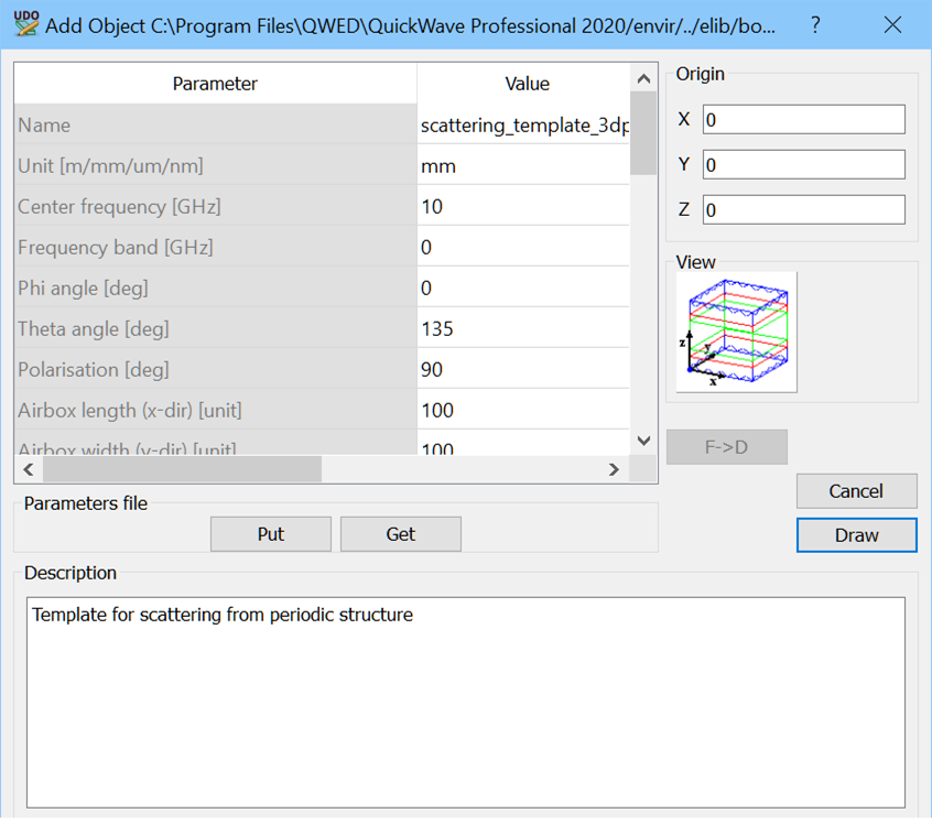
Fig. 2.17.1-6 Add Object dialogue for the scattering_template_3dp.udo file.
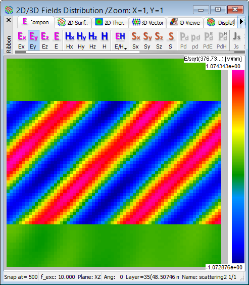
Fig. 2.17.1-7 2D/3D Fields Distribution window for the scattering2 example.
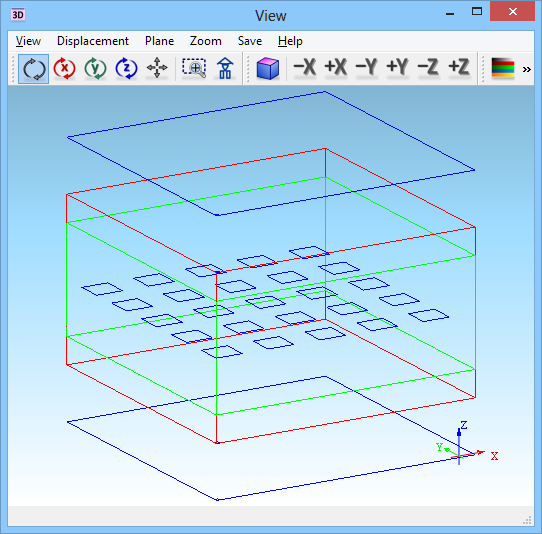
Fig. 2.17.1-8 3D View of the scattering3.pro model.
We consider the PLW illumination of the regularly arranged 10 mm x 10 mm rectangular metal patches (see Fig. 2.17.1-8). Principal period is 20 mm in both directions. Fig. 2.17.1-9 presents the scattering pattern obtained for this scenario. We observe the 0th diffraction order beam at the 450. The higher reflection orders neighbouring the 0th order are not disturbed (see the nulls indicated with dashed lines). Moreover, according to the following relation:
![]()
( 2.17.1-2)
where θ inc is an illumination angle, θm is the mth diffraction order and L stands for the spatial period, we may also expect the presence of the 1st diffraction order at θ1 = –52.40 and indeed there is another beam indicated at the scattering pattern (see Fig. 2.17.1-9).
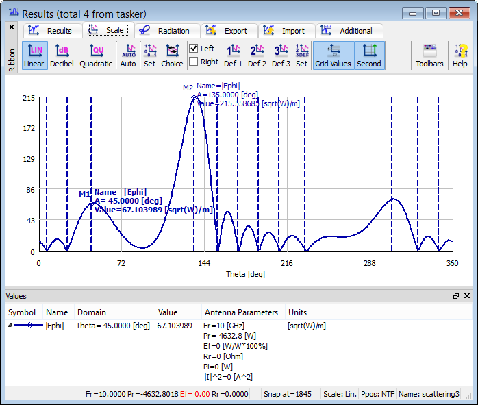
Fig. 2.17.1-9 Results window with scattering pattern for the scattering3 example.
The 3DP circuit type allows to analyse not only the scattering problems but also eigenvalue ones - see Eigenmodes in photonic crystals.