2.11.1 A simple waveguide example
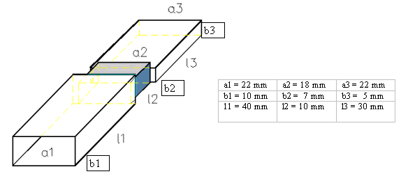
Let us consider a circuit, which consists of a matching section inserted between two rectangular waveguides of different height and width:
Circuit analysis in QuickWave-3D can be divided into nine steps:
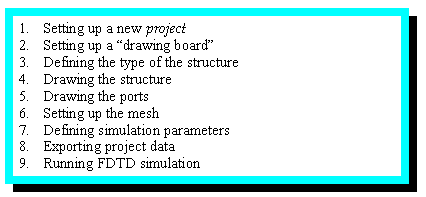
Eight steps are performed by QW-Editor, and only the last step by QW-Simulator.
STEP 1: setting up a new project
On the entry to QW-Editor you will see the last project developed by previous users of the software. Please press ![]() button to open your new project. The default name noname will appear in the title bar. Now select Save as in Home tab, and write the name of your project into a dialogue box; let the name be: my1st.pro.
button to open your new project. The default name noname will appear in the title bar. Now select Save as in Home tab, and write the name of your project into a dialogue box; let the name be: my1st.pro.
Note that the windows of the previous project have remained open. Close the windows you do not need. In fact, you will need at least one 2D Window for drawing, and a few additional 2D and 3D Windows may be helpful for visualisation. Open the new windows either with ![]()
![]() buttons from Home tab of QW-Editor.
buttons from Home tab of QW-Editor.
At this stage you should decide what units will be used. To set the units please invoke Units dialogue (![]() button in Model tab) from main menu, and select an appropriate radio button in the dialogue.
button in Model tab) from main menu, and select an appropriate radio button in the dialogue.
STEP 2: setting up a “drawing board”
In QW-Editor the geometry is defined manually only in a 2D Window in the XY-plane. Thus you should appropriately format at least one 2D Window to serve as a convenient “drawing board”.
The dimensions of your open windows have been inherited from previous projects or determined by default parameters of QW-Editor (depending on the history of your installation). Note that the location within your “drawing board” is shown in the status bar in units that you have chosen.
The dimensions of the “drawing board” can be modified by setting up the axes. From the 2D Window menu press Axes ![]() button, and introduce appropriate values for U (horizontal) and V (vertical) in the dialogue. Remember that Min and Max are the beginning and end of each axis, Step is a step between consecutive ticks. As the outermost dimensions of our structure are 80x22 mm, you can set for example MinU=0, MaxU=80, MinV=0, MaxV=22, StepU=1, StepV=1.
button, and introduce appropriate values for U (horizontal) and V (vertical) in the dialogue. Remember that Min and Max are the beginning and end of each axis, Step is a step between consecutive ticks. As the outermost dimensions of our structure are 80x22 mm, you can set for example MinU=0, MaxU=80, MinV=0, MaxV=22, StepU=1, StepV=1.
If the Visible box is checked on Ú, in the left corner of the 2D Window you see two axis (U, V coloured magenta, brown) of the local 2D system. Even if the axes are not marked as Visible, they force the minimum dimensions of the window (the window will become larger to accommodate elements drawn outside the axes limits).
Attention:
If you inherit from a previous project a 2D Window in a zoom mode, the dimensions of this window will not properly react to the changes of axes. You can eliminate this problem by pressing Extents ![]() button from the 2D window menu.
button from the 2D window menu.
Now press Grid/Snap ![]() button and make your settings. With Grid box marked, you would see (independently of the axes) a 2D grid of small black dots over the window area, which may be helpful in drawing. Snap is even more important. Please always check the Snap box on, and set the value of the snap not lower than the accuracy with which the dimensions in the project are defined. In our case we set snap to 1 mm: StepU=1, StepV=1. Other settings of this Grid/Snap Parameters dialogue are less important in the considered example.
button and make your settings. With Grid box marked, you would see (independently of the axes) a 2D grid of small black dots over the window area, which may be helpful in drawing. Snap is even more important. Please always check the Snap box on, and set the value of the snap not lower than the accuracy with which the dimensions in the project are defined. In our case we set snap to 1 mm: StepU=1, StepV=1. Other settings of this Grid/Snap Parameters dialogue are less important in the considered example.
STEP 3: defining the type of the structure
In the 2D Window, press Circuit ![]() button. Please make the following settings in the dialogue that appears:
button. Please make the following settings in the dialogue that appears:
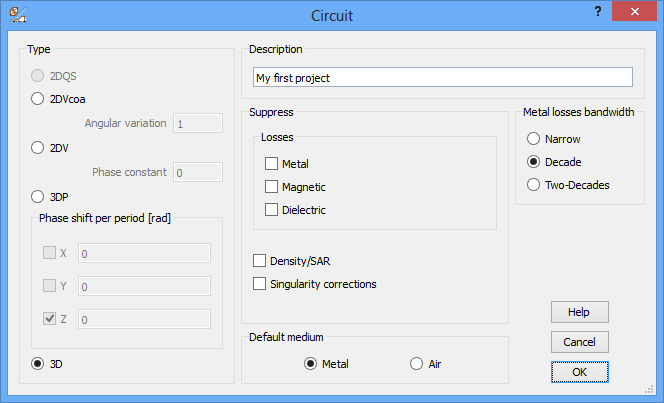
· Check 3D as a circuit type (our structure is three-dimensional).
· Choose Metal as a default medium (this means that we will be ‘drilling’ our circuit in metal).
· Write a short description line, for example My first project.
· Click OK.
Here are some remarks about the options, which we have not used this time in the Circuit dialogue:
· Our structure is lossless so the Suppress losses option is irrelevant. This option is used when we have a lossy circuit, but we want to run preliminary analysis without taking its dielectric and/or magnetic and/or metal losses into account.
· Similarly, the Metal losses bandwidth option is irrelevant.
· The Suppress Density/SAR option is also irrelevant. This option is used when we have a circuit prepared for SAR analysis, with non-zero value of density assigned to some media, but we want to run preliminary analysis without calculating SAR and thus, without constructing density matrices in QW-Simulator.
· We shall return to the Suppress Singularity corrections option at the end of this Section.
· Phase shift per period is active only for 3DP (three-dimensional periodic) or 2DVcoa (vector two dimensional) circuits.
· Regarding the Default medium, the other possible choice is Air. As a matter of exercise: go back to Circuit dialogue, choose Air and click OK. Note that information on the title bar of 2D Windows has changed from *IN METAL* into *IN AIR*. The background colour has changed (unless previous users of your installation assigned the same background colour to both default media). Be careful to restore our Metal setting before proceeding with this project (go again to Circuit dialogue, choose Metal and click OK, make sure that the title bar of the 2D Window is *IN METAL*).
STEP 4: drawing the structure
Before you actually begin to draw, set the base level and height of the first element. Let us begin with the first waveguide. Its height is 10 mm, and let us start at level Z=0. Please call Define Level dialogue (![]() button in 2D Window) to introduce Level Z=0, Default H=10. Since the top and bottom waveguide walls will be a metal boundary, it is advisable to set there E-plane of the FDTD meshing (see FDTD method in QuickWave Software). Thus we also set Bottom/top kind = Electric. Note that the default setting of Medium Name: air is OK for this project. Click OK.
button in 2D Window) to introduce Level Z=0, Default H=10. Since the top and bottom waveguide walls will be a metal boundary, it is advisable to set there E-plane of the FDTD meshing (see FDTD method in QuickWave Software). Thus we also set Bottom/top kind = Electric. Note that the default setting of Medium Name: air is OK for this project. Click OK.
The structure of the circuit is drawn using commands from the Draw menu. Some of the commands can also be accessed by clicking an appropriate button in the 2D Window toolbar:
The broader side of the guide a1 will be drawn along the V axis, the length l1 along the U axis. For this simple shape it is enough to click ![]() on the toolbar (or equivalently, use Draw-Element-Rectangle command). Note that the cursor has changed from arrow into cross. The rectangle will be drawn by fixing its two opposite vertices. Let us place these vertices at (0,0) and (40,22). There are two possible ways:
on the toolbar (or equivalently, use Draw-Element-Rectangle command). Note that the cursor has changed from arrow into cross. The rectangle will be drawn by fixing its two opposite vertices. Let us place these vertices at (0,0) and (40,22). There are two possible ways:
® either with a mouse: move the mouse to a position (0,0); press left button; with button all the time pressed, move the mouse to a position (40,22); let the button go and press it again; now press right mouse button to exit the drawing mode (cursor goes back to arrow);
® or with a keyboard: press K on the keyboard; in the appearing Keyboard Entry dialogue introduce U=0, V=0, click OK (or equivalently Enter on the keyboard); press K again; in the dialogue introduce U=40, V=22, click OK; press right mouse button to exit the drawing mode (cursor goes back to arrow).
The other two waveguide sections are drawn in the same way.
Before you draw the transformer section remember to set new height through: in Define Level dialogue change Default H=7, and click OK. Now draw a rectangle with vertices (40,2) and (50,20).
To define the output waveguide, set height through: in Define Level dialogue change Default H=5, and click OK. Draw a rectangle with vertices (50,0) and (80,22).
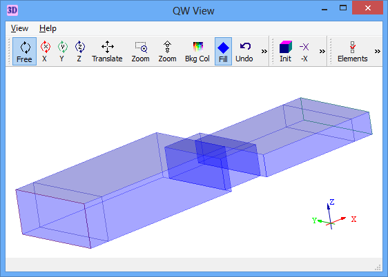
While drawing, please observe the shape in 3D Window wireframe view or 3D Window solid view. In the 3D Window we can see three axes of the general 3D System (X, Y, Z, thin lines coloured green, red, blue) and two axes of the local 2D system (U, V, thick lines coloured magenta, brown).
Back in the 2D Window, press the ![]() button to see the list of elements you have drawn. It is a good habit to consult this list always after you have drawn some new elements!
button to see the list of elements you have drawn. It is a good habit to consult this list always after you have drawn some new elements!
STEP 5: drawing the ports
The next task is to draw ports in the waveguides. Input port will be set in the first guide so please call Define Level dialogue, introduce Level Z=0, Default H=10, and click OK.
Now call the command Draw-IOPorts (or equivalently, press the ![]() button). You will get the I/O ports dialogue window:
button). You will get the I/O ports dialogue window:
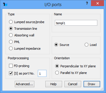
· Check Transmission line.
· Check the box [S] and fill in as port No.1(to include this port in the system of S‑parameter calculations as port number 1).
· Click Perpendicular to XY plane (since our port is in the YZ -plane)
· Click Draw.
Note that the cursor in the 2D Window has changed to cross which permits drawing. You are now expected to draw a line between points (0,0) and (0,22). You can use a mouse or a keyboard, as explained in STEP 4.
Note that checking the [S] box automatically introduces a reference plane situated at some distance from the port. The sources and reference planes are marked by arrows corresponding to the anticipated direction of the energy flow.
Here are some remarks about the options which we have not used this time in the I/O Ports dialogue:
· It is possible to change Port name.
· Port number must remain 1 because this is the input!
Now you can draw the output port.
Call Define Level dialogue, introduce Level Z=0, Default H=5, and click OK.
Now you can proceed as above: press ![]() button check the appropriate options, and draw a line between the appropriate points.
button check the appropriate options, and draw a line between the appropriate points.
However, we also want to present an alternative way, which avoids drawing the line. Select Edit- Line (![]() button); seeing that the cursor has changed into a square, move it with a mouse close to the right-most line of your circuit (where you want to place the output); press left mouse button and move the selected line - just to make sure that you have selected the correct one; release left mouse button and press right mouse button; you will see Line Change dialogue:
button); seeing that the cursor has changed into a square, move it with a mouse close to the right-most line of your circuit (where you want to place the output); press left mouse button and move the selected line - just to make sure that you have selected the correct one; release left mouse button and press right mouse button; you will see Line Change dialogue:
Press I/O port, and you will see again the I/O Ports dialogue. Please make the following settings:
· Check Transmission line.
· Check the box [S] and fill in as port No.2.
· Click radio button Load (very important!).
· Click Draw.
The port is drawn automatically along the selected line. Press E on the keyboard to exit the edit mode (return to arrow cursor).
Note that the absorbing ports are marked by triangles directed towards the direction from which the wave is coming (imitating unechoic chamber walls). If the software puts opposite direction to what you need (which happens very rarely), you can change it through the Edit I/OPort dialogue (accessible by double-clicking the port on ![]() list, followed by right mouse button click; then modify Activity field).
list, followed by right mouse button click; then modify Activity field).
In the 2D Window, press the ![]() button. You can see that the two ports and two reference planes have been added to the list. It is a good habit to consult this list always after you have drawn some new ports!
button. You can see that the two ports and two reference planes have been added to the list. It is a good habit to consult this list always after you have drawn some new ports!
STEP 6: setting up the mesh
Setting the FDTD mesh parameters is an important and delicate operation. It influences the speed and accuracy of calculations. To speed-up the calculations you can lower the density of the mesh, at the cost of accuracy. The biggest admissible cell size is determined by two factors: wavelength resolution and geometry resolution. As a rule of thumb, the shortest wavelength should be resolved into at least ten cells, while the narrowest element – into two cells.
Open Mesh Parameters dialogue (![]() button in 2D Window).
button in 2D Window).
· Because we want the mesh to be created on the entire area occupied by our structure mark in the section Adjust to the default setting: Objects. Thus manual mesh boundaries become irrelevant.
· In the left part of the dialogue box we set the maximum FDTD cell size (Max cell size) along the three axes X, Y and Z. Let us set first 1 mm in all directions.
· Edges force linear mesh is also irrelevant because in this simple example we will maintain regular meshing.
· Check the box Visible to subsequently see the mesh in all 2D Windows.
· Click OK.
Note that the meshing is performed automatically. Open Mesh/Splanes Info dialogue (![]() button in 2D Window) to see how many cells have been created in the QW-Editor and how many will be considered by the QW‑Simulator (including the cells needed to model the boundary effects). Take a look at minimum dimensions of created cells. It is a good habit to consult Mesh/Splanes Info dialogue when the drawing of your structure is complete!
button in 2D Window) to see how many cells have been created in the QW-Editor and how many will be considered by the QW‑Simulator (including the cells needed to model the boundary effects). Take a look at minimum dimensions of created cells. It is a good habit to consult Mesh/Splanes Info dialogue when the drawing of your structure is complete!
STEP 7: defining simulation parameters
Parameters of the simulation are defined through the Edit Transmission Line Port and S-Parameters dialogues.
Press ![]() button from Simulation tab. In the S-Parameters dialogue:
button from Simulation tab. In the S-Parameters dialogue:
· check the box S-Parameters
· set the frequency range: from 7 GHz to 13 GHz step 0.01 GHz
· select reciprocal lossless 2-port
· click OK.
Note that all other default settings of S Parameters Advanced are appropriate for this example:
· checkedSk1 at reference planes means that the software will calculate the Sk1 parameters with excitation applied to one port (source), with template filtering,
· Iterations per port number is relevant only for Smn sequential analysis - thus although we have not changed the default setting 5000, the program will continue simulations until stopped by the user,
· Apply box of the Prony method has not been checked - it would be used for activating an optional QProny module.
· Please also remember that the following S-corrections can be made by the software:
· checked reciprocal N-port means that the circuit is considered as reciprocal – this enables the software to correct S11 for numerical reflections from imperfect absorbing boundary at other ports (loads),
· reciprocal lossless 2-port enables the software to also correct S21 for numerical reflections from imperfect absorbing boundary at the load; the effect of its application will be demonstrated later;
Now open Edit Transmission Line Port dialogue source port templ1. We must define: spatial field distribution in the cross-section of the port and excitation time-waveform.
Let us start with the time-waveform. On the left hand side of the dialogue in Parameters tab:
· Select Excitation Waveformas pulse of spectrum f1<f<f2;
· Set spectrum limits f1=7 GHz, f2=13 GHz;
· Do not change pulse Duration=3 and Amplitude=1.
Now we consider spatial field distribution of the exciting field or in other words - excitation template. Since this port has been drawn as a Transmission line port, the default setting for Exciting field is Arbitrary. This permits to apply excitation with spatial distribution of transversal field components corresponding to any mode of the line.
In the Template Advanced Parameters dialogue:
· Set Matching frequency 10 GHz within 1 GHz.
· Set Template mode searching range from 7 to 13 step 0.4.
· Select the Automatic radio button in the Generation field.
Further, we have a general way and an easy way of specifying the mode of excitation. Both ways will be presented below.
Going the general way the user can obtain any mode of interest, but must excite it:
· at a proper point within the port,
· with a proper field component,
· with correct value of effective permittivity.
The dominant TE10 mode can be excited, for example, with Ez field component at the centre of the guide’s cross-section. The central point is a default setting of QW-Editor. In Template mode search details select Field component Ez; and set periods for field pattern generation to 167.
In the centre, set Permittivity (effective) 0.535. Since we are dealing with rectangular hollow waveguides, this effective permittivity has been calculated with eq.(2.2.4-8); however, we have subsequently chosen to truncate it to three decimal digits. For more information about effective permittivity please refer to First insight template generation.
Going the easy way means that for typically used modes, the software will automatically make the above settings. All the user has to do is to select the desired mode from the list of available exciting field choices. Please make some experiments to see how this works:
· Select R_TE10, which denotes rectangular waveguide TE10 mode - you will note that QW‑Editor has recalculated the effective permittivity with more significant digits, as 0.535767.
· Select R_TE01. QW-Editor has recalculated the effective permittivity as -1.246888 - a negative value means that the requested matching frequency of 10 GHz is below the TE01 mode cutoff. Also, the Field component has changed to Ey.
This is all for the source (if you have been experimenting with the modes, do not forget to restore the settings to R_TE10 mode, resulting in Ez and 0.535767!).
Now click the Next box to see the settings for the load.
Note that since a1=a3, selecting R_TE10 mode again produces the same effective permittivity 0.535767 and the same Ez field component.
Repeat the same sequence of 9 settings (bulleted above) regarding excitation and template with one difference: please set Template mode searching range from 7 to 13 step 0.5. Click OK.
STEP 8: exporting project data
Now we can start the simulation by pressing ![]() button in Simulation tab of QW-Editor.
button in Simulation tab of QW-Editor.
STEP 9: running FDTD simulation
In QW-Simulator the Simulator Log window appears where you can read information about the progress of the analysis:
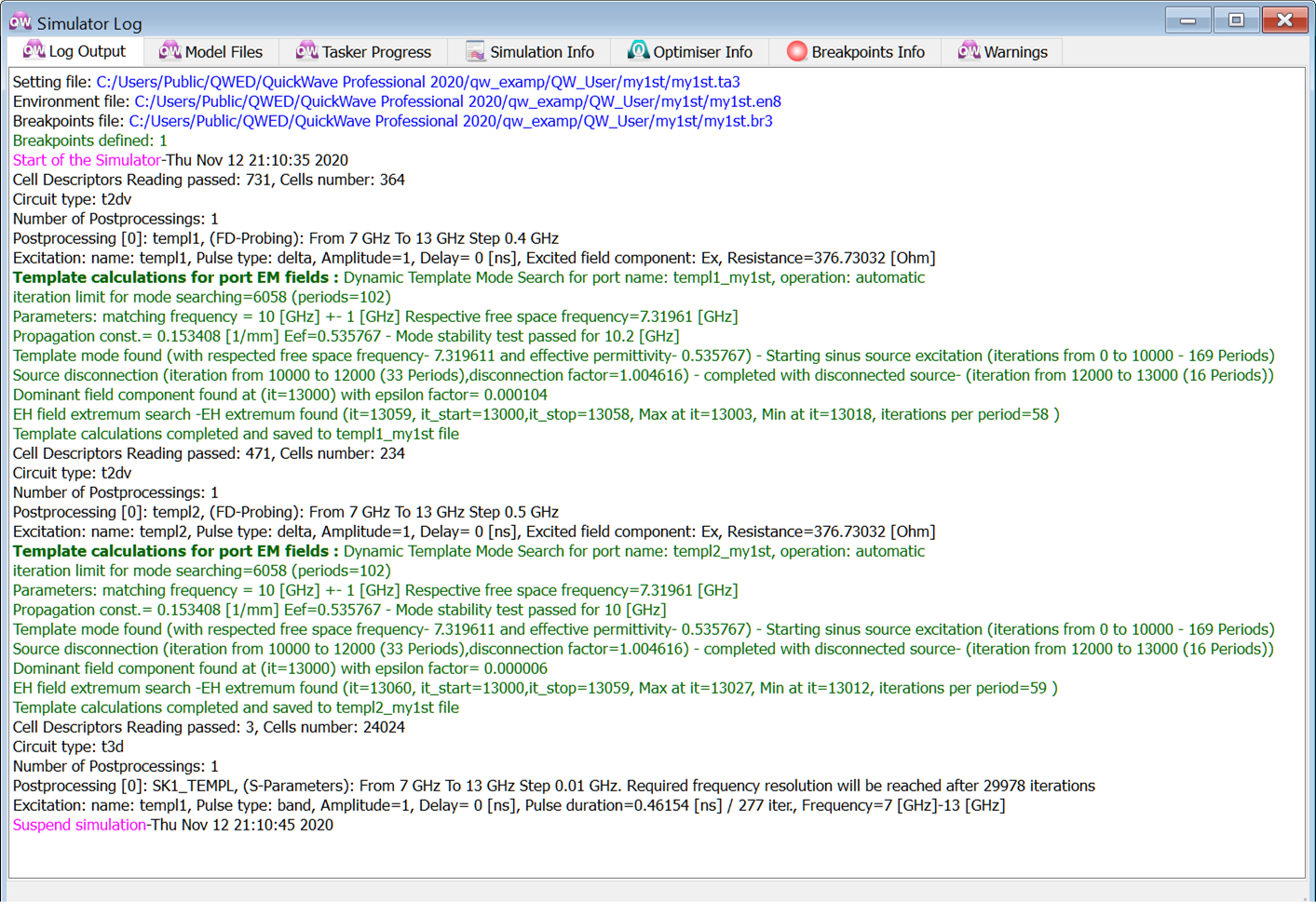
After six lines indicating the start of the simulation, we can see a line stating that at the first port we calculate the template in an automatic way. Then we can read the software has found a mode at the frequency 10.2 GHz. For the second port the mode has been found at 10.0 GHz. The origin of this discrepancy resides in different values step in template mode searching range defined for the two templates in STEP 7. Let us explain this in detail:
From the values of matching frequency=10 GHz and permittivity (effective)=0.535767 defined in STEP 7, QW-Simulator has calculated the value of the propagation constant along the guide. It is equal to the propagation constant of plane wave in vacuum at 10*(0.535767)0.5 » 7.31961 GHz. This is the value displayed in lines started with “Parameters:” of the Simulator Log.
Since the propagation constant is determined accurately, we expect a resonance at exactly 10 GHz, and indeed this is what we have found for the second template. In the first template the template mode searching range was defined (in STEP 7) as: from 7 to 13 step 0.4 so 10.0 is not one of the considered frequencies. The closest one in 10.2, and this has been found. Since we have requested matching frequency 10 GHz within 1 GHz, the value of 10.2 has been accepted by the software.
Note that if the calculated frequency of the mode does not fall within the assumed range, the program changes the propagation constant and tries again. In this case the consecutive propagation constants and frequencies appear in the Simulator Log.
The Simulator Log depicts successive phases of template generation, their duration and parameters. Let us explain the meaning of these numbers:
· As already mentioned, the number 7.319611 is a respective free space frequency – a frequency whereat a plane wave in free space would propagate with the same propagation constant as our waveguide mode, at the desired matching frequency. For more details please refer to First insight template generation, eq. (2.2.4-9).
· Iteration limit for mode searching=6058 (periods=102) means that the first search for the mode will take place at iteration 6058, which is obtained by the software as 0.6*169, where 169 is the number of periods introduced in STEP 7 as limit of iterations, and 0.6 is a constant factor (exception: if 0.6* limit of iterations <1000, this phase would last for 1000 iterations).
· Template mode found (with respected free space frequency -7.31961) - Starting sinus source excitation (iterations from 0 to 10000 - 169 Periods) means that sinusoidal excitation will be directly applied for 10000 iterations, which is the number of periods (169) introduced in STEP 7.
· Source disconnection (iteration from 10000 to 12000 (33 Periods), disconnection factor=1.004616)... means that the source will be gradually disconnected between iteration 10000 (limit of iterations) and 12000 (12000=10000+0.2*10000, 0.2 being a constant factor, no exceptions). At each iteration, output impedance of the source will be multiplied by 1.004616=1020/(limit of iterations).
· Further ...- completed with disconnected source- (iteration from 12000 to 13000 (16 Periods)) means that after the source disconnection is completed at iteration 12000, the software will look for the largest E-field component in the excited cell until iteration 13000=12000+0.1*10000, where 0.1 is a constant factor (exception: if 0.3* limit of iterations <2500, this phase would last for 2500-0.2*limit of iterations).
Having calculated both templates, QW-Simulator proceeds to 3D calculations. You can watch how the waves propagate in the circuit, and how the computed frequency-domain results converge. From many options available in the View menu, let us consider two: the magnitude of the Ez field component and the amplitude of the S11 parameter.
First open the 2D/3D Fields Distribution window to see the field.
Since this is the first time you are running this project, and the my1st.en8 file does not exist, you can see a program default which is the Ex field in Layer 1. The layout of the window (including colours) is read from the qwsim.ini file. (In successive runs of the same project the contents of the 2D/3D Fields Distribution window would first follow the contents of themy1st.en8 file.) To obtain the following view of the dominant mode propagating through waveguide:
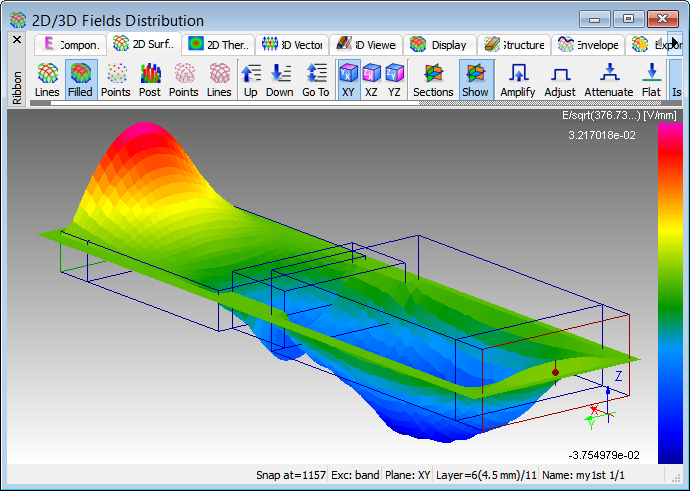
· Click Ez button in Components tab.
· Click the ![]() button to move up (or
button to move up (or ![]() to move down) layer by layer, and
to move down) layer by layer, and ![]() to go to a particular layer.
to go to a particular layer.
· Click the ![]() button to increase (or
button to increase (or ![]() to decrease) the amplitude of the image, and
to decrease) the amplitude of the image, and ![]() to normalise the amplitude to fit into the available window space.
to normalise the amplitude to fit into the available window space.
· DYN in window title informs that the image is being refreshed dynamically, i.e., at every iteration. Naturally, this slows down the analysis. You can switch the dynamic draw on and off either by pressing ![]() button or by pressing D on the keyboard.
button or by pressing D on the keyboard.
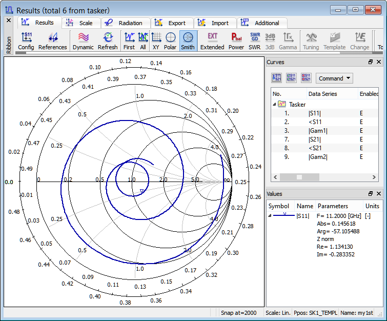
Now open the Results window with ![]() button from Results tab of QW-Simulator. Since the my1st.en8 file does not exist, you can see a program default curve, which is amplitude of S11. The layout of the window and the choice of linear scale are governed by the qwsim.ini file. (In successive runs of the same project the contents of the Results window would first follow the contents of the my1st.en8 file.)
button from Results tab of QW-Simulator. Since the my1st.en8 file does not exist, you can see a program default curve, which is amplitude of S11. The layout of the window and the choice of linear scale are governed by the qwsim.ini file. (In successive runs of the same project the contents of the Results window would first follow the contents of the my1st.en8 file.)
· Press N on the keyboard to see other parameters.
· Press D on the keyboard for dynamic display (results refreshing after each iteration). Press D again to go back to static display.
· Press left mouse to move cursor to new position and get a numerical value of S-parameter at a frequency shown by cursor.
· Press right mouse button to get the floating menu.
· Press space bar to refresh the display.
· Press ![]() button in Scale tab to see the results in [dB]. Press
button in Scale tab to see the results in [dB]. Press ![]() button to return to linear scale.
button to return to linear scale.
· Press ![]() button to see the results on Smith chart.
button to see the results on Smith chart.
· Press ![]() button in Export tab and write a file name with extension *.da3 to save the results.
button in Export tab and write a file name with extension *.da3 to save the results.
The linear and Smith chart displays are shown below. The best matching is obtained at 11.2 GHz where |S11|=0.1456.

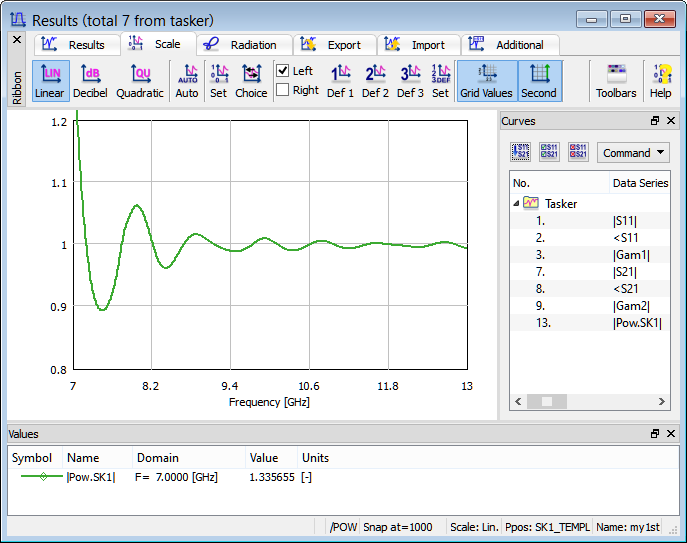
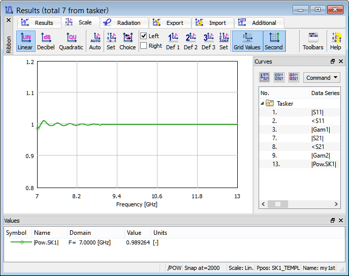
After some time the changes in the result display become negligible, which means that steady state phase has been reached. Also the field values have practically dropped to zero. These are the signs that we can stop simulation. A more rigorous indication comes from watching the power balance, which can be accomplished by pressing ![]() button the Results. For a lossless shielded circuit (with all ports taking part in the S-parameter extraction system), the power balance should converge to unity in the considered frequency band. The following snapshots show the power balance (in the 0.8..1.2 scale) after 500, 1000 and 2000 iterations:
button the Results. For a lossless shielded circuit (with all ports taking part in the S-parameter extraction system), the power balance should converge to unity in the considered frequency band. The following snapshots show the power balance (in the 0.8..1.2 scale) after 500, 1000 and 2000 iterations:

STEP 10: running further experiments
It is strongly advisable to work through this tutorial example a few times changing the mesh, frequency and other parameters to get a better feeling of QW-Editor and QW‑Simulator.
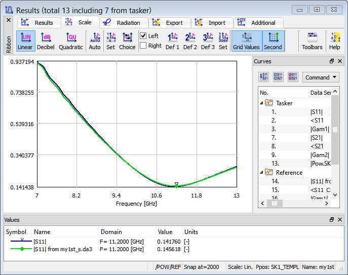
For example, you can watch the effect of field singularity corrections. In this project, the singularity corrections have been introduced by the software at metal corners, in waveguide junction regions. Intuitively, one does not expect these singularities to play an important role in the performance of the structure. Let us return to QW-Editor and suppress the corrections via Circuit dialogue: Suppress Singularity corrections or in Export Options dialogue: Suppress singularity corrections. Running the analysis of this modified project you will obtain the |S11| curve as shown in blue in the figure below. The minimum at 11.2 GHz has slightly changed from 0.1456 to 0.1418. For reference, the results previously obtained with singularity corrections are shown in green (via Load option of Results window). Values and Curves pane was moved by mouse to the bottom of the window. The Values pane is on the top of the Curves pane as indicated by the tabs below the panes.
We can also see the effect of having declared the circuit as reciprocal lossless 2-port. While reciprocity permits to correct the reflection coefficient for numerical reflections from imperfect absorbing boundaries at loads, the lossless flag additionally permits to correct the transmission coefficient in a two-port circuit. Consequently, we can expect better convergence of the power balance.
Let us come back to QW-Editor, open S-Parameters dialogue and check reciprocal N-port. Running the analysis of this modified project, you will see that after 2000 iterations the power balance has converged within 3%, and the power balance curve in the 0.97..1.03 scale looks as follows:

For comparison, let us re-draw the power balance curve obtained previously (with lossless reciprocal 2-port corrections) in the same 0.97..1.03 scale. It has converged significantly better, within 1%:
